
Is there a package file available for the 6.3mm pcb connectors (as seen for example in the above post for +VH, -VH et GND)?
Two 5mm spaced 1mm holes in a 10x6mm casing should do it.
Any better? Are these the good dimensions?
thanks for warning
just add a cap because mister mile diagram doesn't specify a value
just add a cap because mister mile diagram doesn't specify a value
Attachments
Last edited:
Hi, i was wondering if anyone can give me a recomendation? Which amp is better, Symasym, MyRef Rev C, Apex AX16 Bimo mod, or Apex FX8 Bimo mod? The amps that i mention is the amps that i can get easily in my country (Indonesia). Thanks!
Do any of the MJE's need to be on heatsinks?
just transistors wich are in line with output transistors should be on same heatsink.
you should use 2sa 2sc driver transistors as assigned on schematic - I tried to use mj1503x drivers and amplifier tended to go to thermal runaway. with 2sa 2sc drivers all was right.
besides me,you are the first person I know that uses that board. good luck,have a fun!
besides me,you are the first person I know that uses that board. good luck,have a fun!
Scary
Thanx for the info. Will be sure to let you guys know how thigns work out with th build
To confirm, you used the exact same board I used?
What are youthoughts on the sound quality?
What are youthoughts on the sound quality?
yes,I have acomodated it from two boards that Olaf has draw for A14 and A33. Olaf did a great job there,and it was very easy to chop those two into A38 board,since it has two output pairs instead three. A40 has input stage from A33 and output stage from A14,with a little adjustment-take a look at A14 and A33 schematic.
it sounded just as A40 on AlexMM board. just use all transistors as they are assigned at schematic.
it sounded just as A40 on AlexMM board. just use all transistors as they are assigned at schematic.
Last edited:
there were a few simple modes. Mile advised to use 2 of 22p at B-C of driver transistors (easy and best to soldier directly under pcb,althouhg for me it worked without them).
.
there were few schematics with mistakes.
.
first one was 470r marked instead 470k wich actually should be,connected to middle pin od 4k7 offset trimmer. there was no burning with 470r but it was very difficult to adjust offset.
.
another thing is a slight difference between schematics of A33 and A40,there is one less 22r resistor connected to GND.
.
also,if you have 100p at input,iz was advised to change it to 470pF - it will work either way but it will pick up less "noise" with an open output.
.
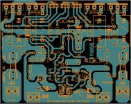
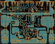
i have assigned all of those diferences at pictures under.
.
there were few schematics with mistakes.
.
first one was 470r marked instead 470k wich actually should be,connected to middle pin od 4k7 offset trimmer. there was no burning with 470r but it was very difficult to adjust offset.
.
another thing is a slight difference between schematics of A33 and A40,there is one less 22r resistor connected to GND.
.
also,if you have 100p at input,iz was advised to change it to 470pF - it will work either way but it will pick up less "noise" with an open output.
.
i have assigned all of those diferences at pictures under.
Attachments


there were a few simple modes. Mile advised to use 2 of 22p at B-C of driver transistors (easy and best to soldier directly under pcb,althouhg for me it worked without them).
.
there were few schematics with mistakes.
.
first one was 470r marked instead 470k wich actually should be,connected to middle pin od 4k7 offset trimmer. there was no burning with 470r but it was very difficult to adjust offset.
.
another thing is a slight difference between schematics of A33 and A40,there is one less 22r resistor connected to GND.
.
also,if you have 100p at input,iz was advised to change it to 470pF - it will work either way but it will pick up less "noise" with an open output.
.
i have assigned all of those diferences at pictures under.
Thanx for all the info. I didnt even know about the two bridge wires marked A and B. I will be sure to make the changes as per your recomendation
Two 5mm spaced 1mm holes in a 10x6mm casing should do it.
Any better? Are these the good dimensions?
Planning to order the drill bits, but don't have the 6.3mm spades yet to measure directly. Is 1mm hole fine or would 0.8mm be better?
Replaced the 470r with a 470k, added 2x 22pf caps per driver transistor, i have the extra 22r resistor to gnd, is this going to be a problem or can I just leave it. And lastly, how thick must the wire connections be from points A and B
make a twisted pair,not too loose and also no need to over-do it. just make sure to connect them as short as you can. I believe that it is not too much problem to leave 22r,but it is not a problem to put short-cut instead. just be careful that you have all right connections according to schematic. picture of pcb in my previous post was the latest I have in sprint6,after I made my pcb.
Planning to order the drill bits, but don't have the 6.3mm spades yet to measure directly. Is 1mm hole fine or would 0.8mm be better?
I use 1.5mm for spade connectors.
I use 1.5mm for spade connectors.
Thanks for the reply.
- Home
- Amplifiers
- Solid State
- 100W Ultimate Fidelity Amplifier