Yes, kind of crazy but should be spectacular sounding or spectacular blowing up in flames. 😀
July 4th already gone...........😀
I would not connect to my speakers with out speakers protection that sure
You should double up the power stage at least
Yes, kind of crazy but should be spectacular sounding or spectacular blowing up in flames. 😀
2 Pair version will be better if voltage is more than 50v. I am working on 2 pair layout.
@xrk can you check 2 pair version on simulation.
Attachments

2 Pair version will be better if voltage is more than 50v. I am working on 2 pair layout.
@xrk can you check 2 pair version on simulation.
Oh nice!
Except that's not an FH9 anymore. It's FH11!
Ok I will look at simulation.
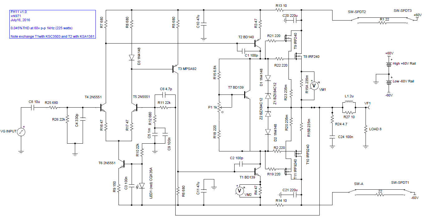
FH11 Tina Sim
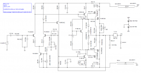
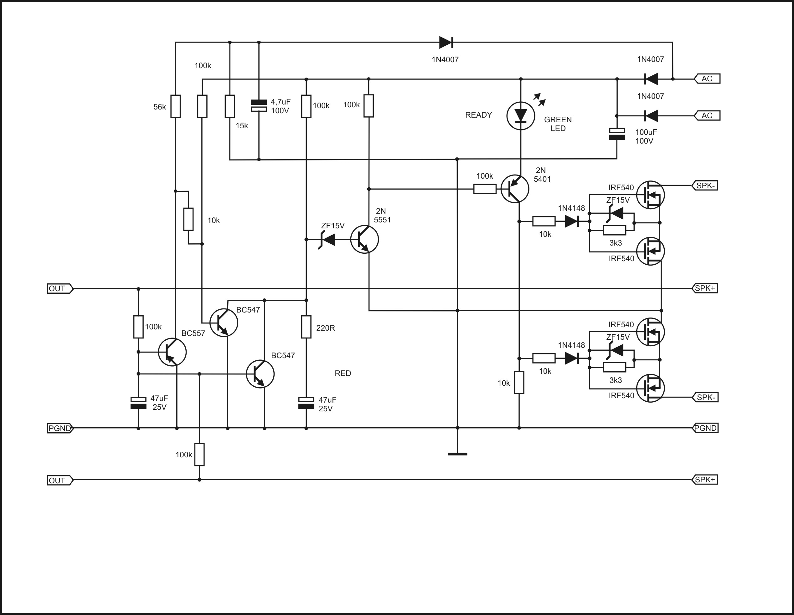
The simulation in Tina looks good, although my library doesn't have either the MJE340/350 or KSC/KSA's - so I used the BD139/140's (over-voltage). The dual 0.47R power resistors are represented as 0.235R in the schematic. I put in an LED for the CCS voltage reference, boosted the power rail caps to 220uF and also added an output Thiele network (optional).
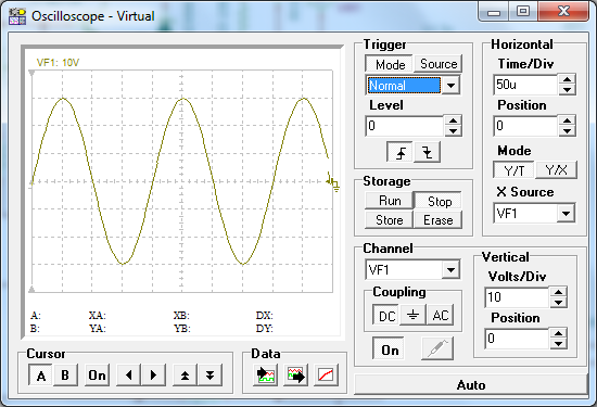
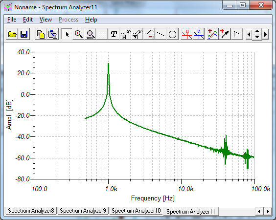
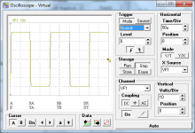
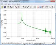
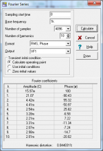
The 1kHz sine wave input (930mV) gives a 60 volts peak-peak output with 0.045% THD. The spectrum looks pretty good, as well as the 5kHz square wave. This is using 175mA bias through each IRFP.
So all in all, I think this amp will work quite well with 2 pair outputs and 60v rails. It's probably good for 225 watts into an 8ohm load.
Schematic:
O-scope sine wave:
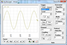
O-scope square wave:

Frequency spectrum:
HD FFT analysis:

The simulation in Tina looks good, although my library doesn't have either the MJE340/350 or KSC/KSA's - so I used the BD139/140's (over-voltage). The dual 0.47R power resistors are represented as 0.235R in the schematic. I put in an LED for the CCS voltage reference, boosted the power rail caps to 220uF and also added an output Thiele network (optional).
The 1kHz sine wave input (930mV) gives a 60 volts peak-peak output with 0.045% THD. The spectrum looks pretty good, as well as the 5kHz square wave. This is using 175mA bias through each IRFP.
So all in all, I think this amp will work quite well with 2 pair outputs and 60v rails. It's probably good for 225 watts into an 8ohm load.
Schematic:
O-scope sine wave:
O-scope square wave:
Frequency spectrum:
HD FFT analysis:
Attachments
Last edited:
There is no capacitor across the Vbe multiplier.
Is this deliberate to get this amp to work well?
How hot have you set the VAS?
It is directly driving the 2pair output stage.
Is this deliberate to get this amp to work well?
How hot have you set the VAS?
It is directly driving the 2pair output stage.
XRK - FH9HV can work on +/- 60DC ?
I Have transformer 2x42V AC
You must use 2 pairs with +/-60DC rails, or class H like H100 with +/-30,+/-60DC... post #54 http://www.diyaudio.com/forums/solid-state/162081-dc-servo-mosfet-amplifier-6.html#post2220363
There is HX11 also class H.
There is no capacitor across the Vbe multiplier.
Is this deliberate to get this amp to work well?
How hot have you set the VAS?
It is directly driving the 2pair output stage.
I'll take a look at the current through the VAS transistors but don't expect it to change much as the Vbe pot was set at basically same position to get same bias current in OPS. The gates on the hexFETs are infinite impedance so the loads on the VAS are purely capacitive.
Apex Audio suggested the two 100pF caps only on the drivers so I never bothered to put it on the Vbe multiplier. It wasn't a matter of trying to get it to work. In fact, the circuit works in the sim (and even the build) without it. Andrewlebon built the version without it and he said it sounds good.
According to the ESP article, T1 and T2 should be swapped so that the hexFETs are driven by the emitter side. The FX8 topology on which FH9 and FH11 are based uses collector side. I wonder why FH9 works as well as it does given the higher impedance of collector follower setup?
A quick experiment by adding another pair might show us if it's possible to use as drawn here. The simulation seems to show some promise.
A quick experiment by adding another pair might show us if it's possible to use as drawn here. The simulation seems to show some promise.
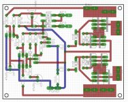
hi, this my first attempt at cad with eagle, so please forgive me
this circuit is in the post 5667 but made one change, parallel irf 540 as suggested from rensil in the post 7692, since i did not know to place the components optimally, i could not finish it in single layer, i need of 15 of those for my lx mini and lx521, (amp is peeceebee v2) ,so i am going to print it any way, so please check for mistakes and suggest changes in detail, please forgive my stupidity if there is any, if its working properly , i will share gerbers
http://www.diyaudio.com/forums/atta...imate-fidelity-amplifier-apex-sst-protect.jpg
Attachments
Last edited:
You are describing an emitter follower driver stageAccording to the ESP article, T1 and T2 should be swapped so that the hexFETs are driven by the emitter side.
If you omit the driver stage then the VAS stays as the common emitter amplifying stage and that alone drives the output FETs directly.The FX8 topology on which FH9 and FH11 are based uses collector side. I wonder why FH9 works as well as it does given the higher impedance of collector follower setup?
A quick experiment by adding another pair might show us if it's possible to use as drawn here. The simulation seems to show some promise.
Most Designers use drivers to ensure the Output FETs see a low enough source impedance. The VAS cannot provide this low impedance.
The capacitive load presented by the FET Gates is a big load on the VAS stage. It gets worse with increasing frequency.
Adding a second pair of outputs doubles the problem of the VAS driving the FETs directly.
21mA of VAS quiescent is unusually high and that is presumably to allow the VAS to drive the FETs.
Look at T2, it too must be passing similar current. Divide by hFE and you get an idea of how much current it's base is injecting into one side of the LTP.
Last edited:
The sim shows 21mA flowing across R4 after T1.
Please post schematic where R4 and T1 are marked clearly !
hi, this my first attempt at cad with eagle, so please forgive me
this circuit is in the post 5667 but made one change, parallel irf 540 as suggested from rensil in the post 7692, since i did not know to place the components optimally, i could not finish it in single layer, i need of 15 of those for my lx mini and lx521, (amp is peeceebee v2) ,so i am going to print it any way, so please check for mistakes and suggest changes in detail, please forgive my stupidity if there is any, if its working properly , i will share gerbers
http://www.diyaudio.com/forums/atta...imate-fidelity-amplifier-apex-sst-protect.jpg
Please post the eagle schematic for ease of checking !
Please post schematic where R4 and T1 are marked clearly !
The schematic is posted in post #8007. T1 and R4 are marked quite clearly (middle bottom of diagram), reposted here:
- Home
- Amplifiers
- Solid State
- 100W Ultimate Fidelity Amplifier