Yes, I have seen this idea.
Even think it was mentioned in forum.
But I can not remember what that power amplifier is called.
There is even a website.
The idea is to have 2 parallel output stages.
One is only used for feedback+correction and the other is the real output stage.
Even think it was mentioned in forum.
But I can not remember what that power amplifier is called.
There is even a website.
The idea is to have 2 parallel output stages.
One is only used for feedback+correction and the other is the real output stage.
Here it is:
The ALTMANN "SPLIF" Amplifier Topology
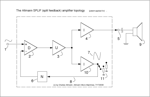
Website: http://www.altmann.haan.de/splif_page/
Lineup
The ALTMANN "SPLIF" Amplifier Topology
Website: http://www.altmann.haan.de/splif_page/
Lineup
So how does this amp handle back EMF?
😀
EDIT:Sorry, I looked at the The ALTMANN "SPLIF" Amplifier Topology pic. Ignor my comment.....
😀
EDIT:Sorry, I looked at the The ALTMANN "SPLIF" Amplifier Topology pic. Ignor my comment.....
Guys,
You make a big mistake ... Take a closer look at the schematic, it is not what you think it is.
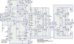
The non feedback output stage, the one which run in pure A classe, is supplied from two 12V PSU and it has a floating ground supplied by output stage of the class AB amplifier.
You make a big mistake ... Take a closer look at the schematic, it is not what you think it is.
The non feedback output stage, the one which run in pure A classe, is supplied from two 12V PSU and it has a floating ground supplied by output stage of the class AB amplifier.
Technics SE-A1 from the late 70s.
Looks great, especially the choice of parts, still waiting for Glen-K to finish his project.
Looks great, especially the choice of parts, still waiting for Glen-K to finish his project.
The circuit was patented by Sano, Hirosha, and Hirota, #4,115,739
in 1977. Personally, I think the concept was a work of art.
😎
in 1977. Personally, I think the concept was a work of art.
😎
Nelson Pass said:The circuit was patented by Sano, Hirosha, and Hirota, #4,115,739
in 1977. Personally, I think the concept was a work of art.
😎
Nelson
I know that you like the circuit, have you built it yet?
I have a copy of the patent; it was first patented in Japan in 1976.
Stinius
Nelson Pass said:Yes I have, and it works as advertised.
It inspired me to patent #5,343,166
😎
Nelson
It’s always good with some inspiration.
Good thinking that cascoded output.
You are using fig5 in you patent as the output I suppose.
Stinius
roender said:Please comment.
I know there is a patent for this type of topologies ...
The no feedback output stage has 2.5A idle current.
The classAB output stage run at 220mA idle current
I don't think this amplifier does what you hope it to. I believe the idea depends on the distortion of both output stages being largely identical. That will certainly not be so with one being a class AB stage and the other being class A.
Think of it this way. If the feedback around the class AB amplifier did a perfect job of eliminating distortion at the output of the class AB stage, then the signal that is fed forward from the input of the class A output stage would contain the inverse crossover distortion of the class AB stage. If the subsequent class A output stage were perfect, all of this inverse class-AB crossover distortion would appear at the output.
This idea, as implemented here, does not appear to work.
Cheers,
Bob
Hi, Bob,
Nice tought. Do you mean signal at junction of R9-R51-C5? I agree that if signal at this point is already contain classAB feedback remedy, than what is fed to classA section also have it.
It will work if the classAB section is also global non-feedback, I think. But classAB needs feedback.
Nice tought. Do you mean signal at junction of R9-R51-C5? I agree that if signal at this point is already contain classAB feedback remedy, than what is fed to classA section also have it.
It will work if the classAB section is also global non-feedback, I think. But classAB needs feedback.
jacco vermeulen said:Technics SE-A1 from the late 70s.
Looks great, especially the choice of parts, still waiting for Glen-K to finish his project.
The topology presented here is not as the Technics A+ patent, which used two completely seperate amplifiers with identical closed loop gain per channel - the class A amplifier with a low voltage power supply for the output transistors only, and the class B amplifier to drive the floating ground of this supply.
Cheers,
Glen
You said so, forgot the long boring discussion you got lured into over your AB stage versus the original ?
More interesting is what you think of Mihai's idea to skip the feedback on the Class A amp part.
More interesting is what you think of Mihai's idea to skip the feedback on the Class A amp part.
No, I never said that. The class B and class A amplifiers are completely separate.
Driving both output stages from the same front-end has the following disadvantages:
1) X-O distortion on the supply rails of the class A output stage is much higher as the class B / AB output stage is open loop.
2) The Class B / AB output stage loads the common VAS and increases VAS non-linearity.
Driving both output stages from the same front-end has the following disadvantages:
1) X-O distortion on the supply rails of the class A output stage is much higher as the class B / AB output stage is open loop.
2) The Class B / AB output stage loads the common VAS and increases VAS non-linearity.
EDIT: I just noticed that it's the class A output stage that is being run open loop, not the class B stage. That makes even less sense.
Cheers,
Glen
Cheers,
Glen
The way the feedback is done in the posted schematic doesn't make much sense at all.
IMO from the output of class A stage would be best, but if you really want the class A stage without feedback then it should be taken from the input of that stage.
Like it is now the feedback tries to correct the crossover distortion from the AB amp which will make the voltage on the input to the AB and A stage have distortion to compensate for that.
- Status
- Not open for further replies.
- Home
- Amplifiers
- Solid State
- 100W A classe with only 45W idle power dissipation