I was just trying to be helpful here.
Yes, thank you.
I might just use a dual footprint that allows the use of the through hole the DIP case for 74HC40105 or SMD. And include provisions to use 32 BCK IIS from 8416 (reminding me to get some modules from Ali Baba and the 40 Schense robbers).
That way, we cover all base's.
You are the brains behind this project and I deeply respect your knowledge and also trying to help make this tda1541 dac progress into something of high-end SQ!
I am expecting to match or exceed the CD-77 with something a bit more simlified.
Please feel free to DM me if I can be of any assistance.
I really need someone with a copy of Proteus Circuit Simulator, which seems the only option including 40105 FIFO models to run some sim's or someone with a link for an unlimited evaluation copy (aka a patched version), so I can test this out.
Thor

OK, but should be tested with shunt-end PS concept for sound.
IME no regulator matches suitable size low ESR capacitors.
metastability...
Is the same kind of magical thinking like the "conversion silence" thing with TDA1541 Sim mode.
It is an urban legend, that results from violating setup time.
Solution, make sure that you invert MCK so the rising MCK edge is always enough after the rising Data/BCK/WCK edge to comply with the flip flop's setup time requirements.
Recklock ALL with MCK - not with BCK.
Why? What do you hope to gain?
We only need to reclock LE.
Our 32 Bit FIFO feeding TDA1541 via level shifters latches new data on the output on the falling edge, but so does TDA1541.
To comply with setup requirements for TDA1541 we clock the FIFO BCK with Q_Bar and TDA1541 BCK with Q of the final clock divider Flip Flop.
No reclocking on BCK or Data, no point. Just level shifing, probably just using resistors.
Now LE needs to have it's rising edge on the rising edge of the TDA1541 BCK. So our LE is latched on the rising edge of BCK. That aligns the LE Pulse that is in the FIFO with timing requirements of TDA1541 and reclocks it.
Each time we divide our clocks by a factor of 2 we lower Phasenoise by 6dB.
So if we reclock IIS BCK with MCK (_Bar to have reliable setup) and divide the resulting clock by 4 we have cut remaining jitter that reclocks LE by a factor 4 or phasenoise by 12dB, compared to reclocking with MCK, presuming our divider logic is low noise.
In normal I2S stream we have 4 cycles of MCK in one BCK cycle.
that is 8 time stripes in one BCK. When ew use just one F-F we have 1:7 ratio and BCK comes out with half of MCK cycle with oposite edge...
When we use 2 F-F ratio of time in one BCK is 2:6 so it is better.
But maybe the best situation is to have 4:4 ratio of time, same rising egdges in the middle of BCK
How much jitter do you expect, for goodness sake?
BCK is too low freq for use as clock for recklocking - almost no sense...
As any categorical statement without reference to the actual use case and without qualifications, this is wrong.
Depends what you reclock. It's perfect to apply the correct timing for LE on the TDA1541 AND also reclock it with the lowest jitter clock available in the system
Much better is to use MCK that is already present.
Absolutely not. Another one of these categorical statements without use case reference.
There is no neeed for recklocking in the output of FiFo
There is on LE.
But there is for the input side.
Partially correct.
Reclock BCK with MCK from USB or WM8804/5 where MCH has lower phase noise than BCK (but not when using AK4118 or CS8416 - as MCK is noisier than BCK). This way we have the lowest phase-noise / jitter in the source at the beginning of the Output BCK Chain.
Again, we first need to analyse the use case and requirements and then determine the best solution, instead of coming with predetermined solution and trying to hammer it into the circuit on the idée fixe that "this is the way to do it".
Thor
We only need to reclock LE.
Our 32 Bit FIFO feeding TDA1541 via level shifters latches new data on the output on the falling edge, but so does TDA1541.
Ok, I updated my timing graphs including the appx FIFO Delay etc. All this is for 192kHz with the IIS BCK Cycle ~ 80nS. The negative spikes on SI/SO are actually up to ~ 20nS wide. Putting this in means I have to redo the whole spreadsheet with double the number of columns.
I'm presuming a really fast (74F74, 74AC74 or 74AUC1G175) Flip Flop for the LE reclocker (take something slow and the setup time may not work).
It shows all relevant edges and data clearly marching into the TDA1541 in correct order and timing.
Where there is a risk of meta stability and/or timing uncertainty I have drawn this in.
As we can see, we can use the first FIFO (the one that stores the left channel 16 Bit Data to align it with the right channel data) can also give all the necessary timing to gate the the SI Clock (input bit clock) for the flow control together with a 1/2 BCK delayed WCK.
We may need to see how the LE & MSB Inversion behaves in the sim. I'm still thinking how it will work best, we need a "cutoff" before the next rising edge of I2S BCK, but some holdup time. Double inverter perhaps.
Here a more detailed schematic of the 74HC40105 internals. It may make it clearer what goes on inside.
Thor
Ok, I updated my timing graphs including the appx FIFO Delay etc.
And I just had a BBFOTFO*.
The relatively slow FIFO's cause some uncertainty and headaches for the project.
The solution, cascade FIFO IC's differently.
First, one FIFO (#0) gets loaded with the 16 Bit's for left. One of the 4 lanes is used. This is done by gating the SI (input) clock so it runs at WCK = L with a delayed clock.
We run the the output of FIFO #0 into the next FIFO (#1) say D0. The actual data from I2S connects to D1. FIFO #0 /SO (output) clock connects to FIFO #1 SI.
After 16 BCK out FIFO #1 holds 16 bit L/R and FIFO #0 is empty. We should actually also enter the LE "marker" into FIFO #1.
There is no reason to use BCK as the output clock of FIFO #1 to transfer data into FIFO #2.
Flow control can be left to the FIFO expansion system.
The logic is simple, while FIFO #0 is empty, we stop SI to FIFO #1 and connect FIFO #1 SO to FIFO #2 DIR, so FIFO #2 can "pull" data from FIFO #1 as fast as it can.
With FIFO #1 full, FIFO#3 will hold 4 bits. The next 12 Bit will ripple into FIFO #3 at the maximum speed the FIFO's are capable of, around 30MHz according to datasheet.
As the final 4 bit of the previous sample and LE are clocked out of FIFO #3 the remaining 4 Bits in FIFO #2 transfer into FIFO #3, which now again holds 16 bit's with the MSB/LE marker.
FIFO #0 and FIFO #1 are empty. WCK goes low, we start again clocking into FIFO #0 and the cascading between FIFO #1 & #2 is cut .
We do inversion of MSB after the FIFO using the LE pulse. We reclock/latch LE with BCK, creating the correct timing for TDA1541.
This minimises any additional logic and relies on the FIFO's internal control for managing most flow control and WCK for the rest.
I think we are zeroing in on a solution.
Thor
I think we are zeroing in on a solution.
Ok, the logic diagram has grown enough to no longer fit vertically on my screen....
I added more colour to make it easier to follow. previous versions had some errors.
Working backwards, from the TDA1541 inputs.
As it stands, we use a pair of 74AC74/74F74 Flip Flops (lowest added phase noise except AUC logic) to divide BCK by a factor 4. This gives our output clock with low jitter and delay.
We add another 74AC74/74F74 flip to re-clock BCK by MCK.
We use the final 74AC74 as latch to correct LE Timing and re-clock the LE with our divided BCK, which is the crucial clock in our system.
We use BCK/4 for the FIFO output clock and BCK/4 INV to clock TDA1541?
We then add more 74HC74 for the DEM clocking. Coming to that later, but 48kHz FS is 768kHz BCK. Divide by 4 for 176kHz, @ 96kHz we get 384kHz DEM (optimum per @lcsaszar) and 768kHz @ 192kHz (with 3.072MHz BCK). A slight compromise, but all these frequencies are "normal".
The final 74HC40105 FIFO of 3 FIFO IC's in the system provides the following signals:
LSB FLAG aligned with LSB
MSB FLAG aligned with MSB
DATA L
DATA R
A pair of 74HC86 gates invert the MSB when MSB Flag = H. We use 1/2 74AC74 to use the LSB to derive the LE pulse from it.
We use resistor dividers / pullups with ~ 3kOhm output impedance ( ) to give reduced signal swing and slew rate limiting (36nS rise time to 70% of 1.8V) for TDA1541. Very simple. For LE we make a "flying" attenuator. Ok, Last FIFO and TDA1541 are taken care of.
The FIFO before this is connected as extension. I need to think a bit more if we need extra flow control here of just let the final FIFO "pull" data as it comes out. On a quick think I see no reason to stop new data to go straight to the output FIFO if there is space. The Input of this FIFO get's it's Data inputs from the next section.
Now comes the really interesting stuff.
We use 74HC74 (both flip flops) to delay the WCK (1.5 BCK) and an XOR Gate (1/4 74HC86) to get the MSB marker that get's into the first FIFO (FIFO #0) D1.
We use inverted BCK (1/4 74HC86) to invert BCK and one of the delayed (and inverted) WCK to drive a 74HC161 counter that creates the LSB Marker from the 74HC161 TC output to FIFO #0 D0.
I2S Data enters into D2 and D3 is unused (tied High).
Once 16 Bit's of Left Data are latched into FIFO #0 together with LSB and MSB flags we stop the input clock (2 X 74HC08) by using an OR of FIFO #0 DIR and the delayed and inverted Word clock, to gate BCK using a second 74HC08 Gate.
The SO line of FIFO #0 and the SI line of FIFO #1 are linked.
The delayed WCK and the DOR line of FIFO #0 are OR'ed (2 X 74HC08) to enable the BCK to drive these two lines.
On the rising BCK edge Data and Flags on the output of FIOF #0 and the I2S Data line data bit are clocked into FIFO #1.
The falling edge of the gated BCK updates the outputs of FIFO #0, the new word takes on average of 36nS to appear, fast enough to be there before the rising edge. But because we have an interlock with DOR of FIFO #0, if necessary the SI clock is delayed until FIFO #0 has valid data. Once FIFO #0 is empty the clock is stopped.
The system now waits for the WCK falling edge to enable data going into FIFO #0 and everything starts from the beginning.
The nice part is that I think I can simulate all of this in TINA without 40105 models.
IC's to be used:
74AC74 X 2 (TDA1541 Clock divider, BCK & LE Reclocker)
74HC40105 X 3 (FIFO's)
74HC86 X 1 (MSB Inverter, BCK Inverter, MSB Flag generation)
74HC74 X 2 (WCK Delay, DEM Reclock)
74HC08 X 1 (BCK Gating)
74HC161 X 1 (LSB Flag generation)
So 10pcs of 14...16 Pin IC's.
All of them can be using DIP / SOP or TSSOP multiple Footprint and allow a few logic family options.
So again, if someone can look at logic timing diagram and see if I had a brainfade and got something wrong....
Thor
I took couple of scope shots from my STM32H7 USBI2S sim16fs output. FS is 96kHz, channel 1 plays 0xA5A5 and channel 2 0x5A5A. As can be seen with 16fs there is not much timing room for LE. According to datasheet the separation of BCK and LE edges could be 0ns but I doubt that could work with 16fs. The 7ns on my board is probably sufficient.
Attachments
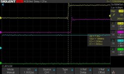
As can be seen with 16fs there is not much timing room for LE.
Really? Rising edge of LE should align with the rising edge of BCK, the TDA1541 in SIM mode loads data on the falling edge. Realistically, the LE rising edge must happen before the following BCK falling edge.
So after the falling edge of BCK we have 1/2 BCK to use a latch to the LE pulse with the rising edge. At 192kHz FS this is 162nS...
The 74AC74 or 74F74 I intend to use have around 3nS propagation delay from CP to Q.
To me, tons of timing room.
There are jobs for software on 32 Bit MCU's with non-guarateed timing.
I think digital audio is better using a realtime system with hardware equivalent timing (e.g. Transputer), or hardware.
Thor
Ok. I seem to have misinterpreted the datasheet as it is not very clear on this. I need to change the register controlling the data sampling edge from rising to falling.Rising edge of LE should align with the rising edge of BCK, the TDA1541 in SIM mode loads data on the falling edge.
The I2S timings of STM32 MCUs are quite well guaranteed. Propagation delay limits or part-to-part skew of 74xx74 is not very tight either.There are jobs for software on 32 Bit MCU's with non-guarateed timing.
but the discrete logic is the whole point of the exercise.No need for any discrete logic.
Ok. I seem to have misinterpreted the datasheet as it is not very clear on this.
Really? Here from the datasheet:
I thought is pretty clear.Fig. 7 shows the second possible input data format. In this mode the DATA signals of the left and right channel are applied simultaneously to two different input pins. Only one bit clock signal is used to clock both data signals into the converter.
The positive slope of the latch enable signal is used to indicate the end of the data input action and to determine the moment at which the outputs change their sample values.
This input format is especially suited for those cases in which the circuits in front of the DAC use a nonstandard serial format.
Yes, this thread has a deep stench of NIH.
Really? Why?
Why should everyone use an STM32 MCU USB to IIS/PCM/SIM bridge without IIS or SPDIF input for their DAC's just to please you and big up your ego?
There are many ways to do a specific job, you offer one option, which once it fully debugged and tested with a real TDA1541, anyone who wants to, will be able to use.
I will probably not use it, for a variety of reasons (not the least lack of SPDIF and IIS inputs options), but hey, not everyone does what I do.
For me doing it differently from how it has been done so far and in the precise way I want to is reason enough.
It's an exercise in design following the concept to get what I want with what I can get and explicitly without code, compiled and CPU as I am doing enough coding as is and am sick and tired of looking at a code screen.
Thor
That board is a multifunction, multichannel board that would suite any DAC users, not only TDA1541. Besides the number of people using SPDIF or I2S input is much lower than those using USB input. But since it is not your design you choose to use Amanero which is outdated and has performance issues.Why should everyone use an STM32 MCU USB to IIS/PCM/SIM bridge
By now it should be clear to everyone which one of us actually needs to constantly boost his ego.ego?
But since it is not your design you choose to use Amanero which is outdated and has performance issues.
Ha, you are incorrect.
Just like now "CS8412" is the standard "footprint" for Chinese SPDIF input modules, using any number of actual IC's, including WM8804 AMD AK4118, "Amanero" is basically a generic footprint.
I just ordered a module for testing that is "Amanero" footprint, but uses QCC5125 as 96/24 USB input and for Bluetooth, including SPDIF out (< 15 USD ready to run).
So together with a WM8804 on "CS8412" footprint (also < 15 USD) we have a good all around input for a DAC intended to complement a TV and/or Android Box.
Add an 8 x TDA1387 DAC Module (< 6 USD), Veroboard, and some supercapacitors plus inductors and regulators, we have a semi decent, very flexible input DAC that meets my personal ideas of "good sound" and is easily replicated as a "DIY" project by a lot of beginners.
I actually want to test CS8416 in slave mode with 32FS BCK, but realistically I need an audio output to be sure. So I decided on a simple "proof of concept".
Anyway, when I write "Amanero footprint" it will actually be a XMOS based module with Accusilicone clocks, but the point of Amanero Footprints x 2 and a CS8412 footprint is that it's easy to get a huge range of different modules.
Now, allow me to suggest that if you want to promote your solution, you do so elsewhere.
I don't come into your threads and then dump on your ideas. Thank you for your consideration.
Thor
The TDA1541A datasheet contradicts the above. The minimum time for both falling edge BCK to rising edge LE and rising edge BCK to falling edge LE is 0ns.Really? Rising edge of LE should align with the rising edge of BCK, the TDA1541 in SIM mode loads data on the falling edge. Realistically, the LE rising edge must happen before the following BCK falling edge.
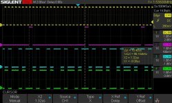
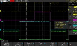
With BCK continuous at 16Fs yields LE as short as what is shown below.
The TDA1541A datasheet contradicts the above. The minimum time for both falling edge BCK to rising edge LE and rising edge BCK to falling edge LE is 0ns.
Correct, the MINIMUM time. Not the ONLY time.
When designing serial logic it is best to leave some space.
I probably wrote this a bit badly, I did not mean to imply that this is a hard requirement, but an easy way to ensure that all timing requirements of the TDA1541(A) are fulfilled.
The hard requirements are that the rising LE edge doesn't happen BEFORE the falling BCK edge of the LSB and that it happens before the next falling BCK edge.
Placing it right into the middle of this window, given all possible timing uncertainty etc. seems commonsensical to me.
There is no limit to the length of the LE pulse, other than it must be low for the required setup time prior to it going high. So making it 1BCK long again is commonsensical and simplifies the circuit.
Thor
Earlier in this thread (in post #66) another member asked me to post a picture of the SIM signals of my board. Doing as asked is not promoting my solution.Now, allow me to suggest that if you want to promote your solution, you do so elsewhere.
Also the datasheet I have is for TDA1541A and has the same diagram as shown above in post #135. That diagram is not very clear which caused my misinterpretation.
The title in this thread asks for collaborators. Usually it is best to have alternative solutions available in case things do not go as planned. Another reason for alternative solutions is that needs vary. With solution as my board those using only USB do not necessarily need any additional board but they may still be interested in both solutions. And if my board is not satisfactory it should be possible to implement similar functionality to @eclipsevl's York boards as implementation on STM32H7 was trivial.
I think I see the issue here. You are approaching this in a, for the want of a better word, rational manner. You see the destination and offer a most efficient way to get there. But this is not that kind of situation. It is like a cycling tour on a penny farthing or a unicycle. The how of getting there is at least as important as getting there. Offering a sleek new BMC will not be greeted with thanks.And if my board is not satisfactory it should be possible to implement similar functionality to @eclipsevl's York boards as implementation on STM32H7 was trivial.
I don't come into your threads and then dump on your ideas. Thank you for your consideration.
Thor
Well , this is exactly what you did on the John thread 😎
.
The title in this thread asks for collaborators. Usually it is best to have alternative solutions available in case things do not go as planned. Another reason for alternative solutions is that needs vary. With solution as my board those using only USB do not necessarily need any additional board but they may still be interested in both solutions. And if my board is not satisfactory it should be possible to implement similar functionality to @eclipsevl's York boards as implementation on STM32H7 was trivial.
One key issue for me is the absence of SPDIF or I2S input's. That is instantly a dealbreaker. So what you offer is to me not a solution.
As stated, I could implement all this trivially in an XU216 where I have most code available including SPDIF and IIS inputs, but I want to do without coding.
So my requirements are simple. IIS in and SIM out. And the Three No's. No CPU, No FPGA, No code. Because my screen looks like this right now:
I want hardware as an antidote.
Thor
- Home
- Source & Line
- Digital Source
- Simultaneous output Frontend for TDA1541 (and or Universal Multibit DAC) using discrete logic - Collaborators wanted