Hi, have to admit I abandoned the project for a while now but I will finish it. Many other non audio things came my way.
Never had built or used anything balanced till about 1 year ago (late adopter 🙂) and as you can see pin 1 was not connected in this test phase. Casing is only connected to PE as it is made of metal. I think when I connect pin 1 of both XLR connectors to casing/PE and reference GND to PE with a resistor it will be silent. Assumption!
Never had built or used anything balanced till about 1 year ago (late adopter 🙂) and as you can see pin 1 was not connected in this test phase. Casing is only connected to PE as it is made of metal. I think when I connect pin 1 of both XLR connectors to casing/PE and reference GND to PE with a resistor it will be silent. Assumption!
Last edited:

Hi ! Try to put 0.9-1V to PLL_AVDD pin with additional regulator. You should cut 0.9V from VDD. There is very low consumption, so you can take input for reg directly from 5V. You'll get sound x2.

It's very simple with small LT3042 board (don't forget to adjust voltage by correct resistor value). I've check it on XMOS U8, XMOS XU208 and here will be the same situation I think. All of them are need very clean analog power for PLL. You can take an oscilloscope and look at that clean power from DC-DC PWM converter at 0.9V.

That LC filter is far from "very clean power supply" and DC-DC converter is also definitely not clean power supply 🙂
It's very simple with small LT3042 board (don't forget to adjust voltage by correct resistor value). I've check it on XMOS U8, XMOS XU208 and here will be the same situation I think. All of them are need very clean analog power for PLL. You can take an oscilloscope and look at that clean power from DC-DC PWM converter at 0.9V.
That LC filter is far from "very clean power supply" and DC-DC converter is also definitely not clean power supply 🙂
This issue is caused by simplified power schematics, in this DAC chip that cap size doesn't matter if you will put good reference 5V to only Vref pins from independent regulator.I changed the Vref caps to the double size and found that as important as the power source.
Last edited:
Yes of course. And I also assume that a really good reg to the pins would be even better. But this was the simplest way for a quick improvement...
OK so you say: don't do a filter but hook up a LT3042 and of course cut the previous PLL-AVdd supply?
Did you do this in your SU-1?
//
OK so you say: don't do a filter but hook up a LT3042 and of course cut the previous PLL-AVdd supply?
Did you do this in your SU-1?
//
No, but I can, I have such one but don't use it. I did it on two another XMOS boards and it brings awesome result. XMOS in SU-1 has the same requirement according to datasheet. I'm not lazy today, so I make a photo of clean power at cap near PLL_AVDD pin at SU-1. Just try my advice upper and you will be surprised with your device.Did you do this in your SU-1?
Attachments
I think I will have to try this - it makes sense.
But 905mV nor 5mV seems to impressive...
//
But 905mV nor 5mV seems to impressive...
//
Last edited:
Sorry but IMHO it only makes sense to mention this when carried out in reality in SU-1. All benefits as experienced in similar but not the very same devices aside no one will be happy when stuff does not work out well in reality for whatever reasons. Please test before publishing.
Of course I will check when I have the time but for now I see a linear 0.9V regulator (and a 1.8V and 2 x 3.3V ones) on the PCB of SU-1.
Of course I will check when I have the time but for now I see a linear 0.9V regulator (and a 1.8V and 2 x 3.3V ones) on the PCB of SU-1.
Last edited:
You don't believe to oscillogram ? Not all IC's in sot23-5 case are linear regulators 😉for now I see a linear 0.9V regulator
I see here LC2202 2A 2MHz 5.5V Synchronous Buck Converter, marking GU then numbers year/weak. It is very easy to find pdf
Last edited:
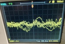
Sorry, I cant really interpret your oscilloscope picture. The scales indicates mV and the screen is more or less half full so we see some traces indicating mV level disturbances on what I interpret is what is present between ground and PLL_AVDD when a LT3042 is connected - if so, its not very clean. Is this scope picture really with a LT 3042? It seem dirty. On a scope that should be a straight line if clean. But we would like to se uV and not really possible to measure with a simple scope in the first place...You don't believe to oscillogram ?
How is it?
//
This is a picture of dc-dc converter supply at PLL_AVDD pin. Neighbor VDD pin is a supply of processor coreIs this scope picture really with a LT 3042? It seem dirty
This is modification of XMOS. I don't need to prove something to someone, but you give me a very good advice at this forum, so I think I should share some good advice with you, so all is working as expected. (Main external power supply is linear 5V 7805 and vref/vddl/vddr are supplied by two LT3045). This is not personal my SU but my friends, so I've checked this XMOS tweak also for him, despite the fact that he doesn't need this device eitherI don't believe a modification that has not been done to SU-1.
Ah that is not what you wrote earlier. Is that 0.9V regulators output really dirty? So it is a switcher putting out 0.9V just for the XMOS? Using and LC filter from pin 27 of the XMOS to pin 22? And how does the new board perform versus the old situation? What about using 2 linear regulators for both 0.9V supplies then?
If the connector block there also carries that needed 0.9V then a small PCB with extra regulator seems better than long wiring (can't be OK in such an environment). I can make such a small add on PCB even if it just would be for mounting and not electrical purposes.
BTW why buy DACs not to use them? Of course one can do without, one can do without audio as a whole too 🙂
Thanks for the compliment, I return it by saying thank you for the added information. When stuff is improved all is good. It just needed a bit more text for correct understanding.
Last edited:
Yes, oscillogramm at photo. And that LC filter is far not enough to make it clean ))Is that 0.9V regulators output really dirty?
Yes.So it is a switcher putting out 0.9V just for the XMOS? Using and LC filter from pin 27 of the XMOS to pin 22?
More sound, cleaner, details, bigger soundstage, deeper soundstage and so on. CPU core doesn't need clean power supply, so that dc-dc is enough for it (also here is big consumption, so any linear regs will be very very hot on this so big voltage drop).And how does the new board perform versus the old situation? What about using 2 linear regulators for both 0.9V supplies then?
He played enough with it and buy much expencive one with another DAC chip and I have another DIY version of AK4493 with much better power supply and layoutBTW why buy DACs not to use them?
BTW this is not a tweak or modification at all. It is just normal power supply where it must be.
Last edited:
So when you wrote "clean" above you where sarcastic?I'm not lazy today, so I make a photo of clean power at cap near PLL_AVDD pin at SU-1.
I think your language skills dont have room for fancy expressions and thus, you might be misinterpreted quite a lot... maybe stick to simple plain english?
Anyways, thanks for the tips!
//
Of course 🙂, I think you'll understand me. Sorry for my language, my english is only at school level, sometimes I use translator, but mostly not.So when you wrote "clean" above you where sarcastic?
Frankly I was confused. Also in other places from you. Please write simple and straight forward - it will be better. Thanks!
//
//
What about trying out another coil? Yes PSU should be good. It still is a tweak/modifcation as it apparently is not good enough like it is done by SMSL.Yes, oscillogramm at photo. And that LC filter is far not enough to make it clean ))
BTW this is not a tweak or modification at all. It is just normal power supply where it must be.
TNT is right in his observation. We can not read between the lines (that you write in your head) or correctly understand vague expressions. So we have a picture showing a supply line but no picture showing the improved supply line which is described as "much better'. Nothing can be concluded, the reader must guess what is meant.
Anyway I think I will make a tiny plug in PCB for TPS7A2009PDBVR just to try out.
Last edited:
Don't waste your time with any coils, that rail is very dirty. Just desolder one coil and put 0.9-0.95V at 22pin (according to datasheet absolute max value is 1.05V but in my case it works great with 1.0V, with LT3042 it's very simple to find 10K resistor for 1V for it's adjustment)What about trying out another coil? Yes PSU should be good. It still is a tweak/modifcation as it apparently is not good enough like it is done by SMSL.
good variant for it's priceTPS7A2009PDBVR
Last edited:
Good idea with 1.0V LDO for both rails, but CPU don't need it, you'll get clean power to CPU and PLL but have some interferences from CPU work.from 1.8V step-down with 1.0V LDO , then to PLL_AVD via a 5.2Ω resistor + 4.7uF ceramic capacitor
Yes, CPUs don't need very clean 3.3V and 1.0V (only PLL need to be clean), but with LDOs the CPU produces less noise (both conducted and radiated) outside.
Anyway, I've used this in dozens of XMOS projects and it works great.
I used the 1.8V step-down converter before 1.0V LDO only to reduce power consumption and heat dissipation.
In some projects, a linear LDO (1117-1.8) was also used instead.
3.3V was always 1117-3.3
I think using LT3042 and similar LDOs in digital circuits is complete overkill.
Alex.
- Home
- Source & Line
- Digital Line Level
- SMSL SU-1 design idea