It ain't necessarily so. Schematic entry is still an option.
I have not worked much with CPLD, just a range of MCU's and CPU's (e.g. XMOS).
My experience is that leaving anything to the compiler is a disasterous choice.
Often critical stuff must be done in Assembler (can I categorically state "I hate Assembler").
So I have my concerns about schematic entry into such tools (Let's all in unison say "Arduino") that hide all the complex and "nasty" stuff from the "programmer".
But that's just me, old, obsolete and suspicious of AI...
Thor
I looked at Pedja Rogic's reg shematic for the chip, serie as far I undesrtand.n Btw sounds good to me, still the ref over what I heard there with DIY. He 's though using shunt stabilizer for the analog i/V section.
Then not related : AD1862 with on shelf regs, very good too but second (better if not difficult frontend).
Could yoy please guys for the didactic or not, but at least pedagic , why the sunt 'stabilizer" is prefered, at least for daxc ics' ?
About driving, which cap has the last word ? the 330 uF efore the ic pins ? All what done before is about lowering output capacitance ?
I try on a basic, and sorry for the digress, why some PS makes better snappier sound, at least on the post current ouput (I/V, ....) ! Phase' ? Something else ?
Sorry for the digress, seems to me the bases, but not sure what to choose diy related !
Hi I put 330uF at the end of sunt because I checked for minimal ESR. Found some recent type, availabile... It is not a big value shunt will spend fast stored energy on shut down. I have to find some apropriate L. I will try to avoid custom made , with first take a look in the official stores. And give some more options for the shunt. to be used or not with elements just populated or not... It is few elements around the tl431. This will not complicate a lot basic circuit without demanding significant further space.About driving, which cap has the last word ? the 330 uF efore the ic pins ? All what done before is about lowering output capacitance ?
Yes the same circuit it is present in My shunt regulator I already posted. (I tried it in praxis before in some +- PS and it perform very good.)Personally I now use the SXST as standard regulator circuit (shunt or series), with RC filtered TL431 as reference:

As there is internal feedback in the TL431 and the SXST I cannot really claim "non-feedback" but in practice for series regulators the result is the same, but with a near zero thermal drift.
.
I will try it as pass transistor unit and put some additional BJT in the base. Used before in pre-regulators triple BJT but in the darlingtom mode. (I remember once I used MPSA18-BD135-TIP31 triple darlington as pass transistor with Vce of 3.5 to 4 V, with 431 as zener.)
.
With "feedback" in termss of regulator I meant taking the sample voltage for the reference zener before and after the pass transitor. I spot earlier that some older power supplies from devices that I love the sound, using very simple regulators, with taking the reference for zener before the pass transistor - without that kind of "feedback" 🙂
.
It is good for testing the unit without the load. In these sircumstances all of the cureent (and one that load will consume) will be going trough the shunt medium power transistors. It must be stabile and without over-heating in these terms.Why do we need equal distribution of dissipation?
And even if for some strange reason we do, given that each supply draws different currents your approach doesn't work anyway, -15V > -5V Shunt always has more dissipation. Design for it (bigger heatsink).
Thor
And with load it will be less heat at the devices and on heatsinks. The goal is to have as less as posibile heat in the interior.
Third reason is to have heatsinks all from the same dimension is to make easier maipulation of PCB and to have stabile and compacet surface wnen soldering etc.
And we can add the phisical look too.
And to have less different parts with say 3 diferent heatsink type you have 3 parts actually n the list...
.
And 6. reason is someone can have -10V for powering BJT IV unit. That will be useful for using tube output to have smaller value of negative grid bias. And to have more options for tube chouce. For instance 5687 needs about -6V to -7V, that will be aprox. value after the Riv dc drop...
Simple more options in the field.
Yes You have 2 options, one with say battery supply with supercaps, and one I send with "opposite" smaller values of capacitors.Basic question :: Is there a possibility to proceed w/o the Farads cells/supercaps
Attachments
I already have some BJT iv for AD1856, 62, 65, and PCM63 dac types. All with "negative" rail Riv.Then not related : AD1862 with on shelf regs, very good too but second (better if not difficult frontend).
And I will post it here or in the topic about AD1862. For AD1862 it is very good beacuse it can use +-12V (or bit higher until max, allowed) of alrady present analog supply. 🙂 I did it to-92 and SMD versions. And the shunt PS for these IVs...
.
Long time ago I adopt some solutions from the topic about BJT ivs. Sergio Santos @SSerg has some similar solutions as Thorsten for positive PNP circuit, but Calvin @Calvin come out with one elegant solution with CFP NPN for negative rail Riv placed. I dont know by heart link to place... sorry.
.
I spot this as good possible solution for TDA dacs and rearange. So it is not out of the blue that i transcribe this IV. The level of "simplicity" is say the same. Same chrs are that JFET at + rail has more than -10db lower noise floor, easy to adjust offset to 0mV, good low value of distortion.
.
I had a idea for one intermediate IV circuit, with good behaviour with lower Riv values - and to use tube after that. to amplify the signal and bring back the phase to 0deg.
All this with direct coupling tube (without need for coupling C), because we have negative grid bias value already.
.
That main circuit, between Io and Riv, could be cascaded for even -20V, -30V or more, if it is to be used with tubes that has l much more negative grid bias.
.
Take a look before few pages i posted a schematic with 2A3 tube to illustrate the idea. 🙂

I set to compare some recent IVs. Common chrs are
(I will left with better tuning of currents trough the transistors, maybe it could be some additional infos?)
(The transfer is a bit cutt-down but it can be eztended with smaller values of C parallel to Riv)
.
That fature with lower Riv values is essentioal. I tried in the past numerous "positive" BJT IVs, that has opposite chr - much worse THD and harmonic order within lowering value of Riv. 🙁
.
FFT is set to: 21ms time, from 1ms, step 100ns. So it takes a bit longer... These are abstract power suplies, but even just with a shunt end results are not significantly degraded. So PS for this type of is also a factor...
.
In the case of connecting the vacuum tube after IV wi "see" ony Dynamic capacitance of the anode follower stage of about 50-100pF say, which is sma compared to present...


- low ditortion for almost all values of Riv. From 33ohms to 1500ohms - about 0.0083%. The best performing with lower Riv values, harmonic content is better. With high value of Riv 5th 6th and 7th harmonics and other H above rising... Just the same as aready happening with the DAC chip and this wi not cance each other 🙁
- easy to adjust zero off-set.
- dependance over the type of CCS from + rail. Best resuts are with JFET and this one with 2 x 1200uF @ base of BJT ccs.
- with higher Riv value, which is the cca. = output resistance, not tolerate "smaller" values of load as 100K. When used alone without buffer.
- shifting phase -180deg (when used as stand alone without inverting buffer.
- the circuit performs almost with amost every easy avaiabe to-92 type of small transistors very good.
(I will left with better tuning of currents trough the transistors, maybe it could be some additional infos?)
(The transfer is a bit cutt-down but it can be eztended with smaller values of C parallel to Riv)
.
That fature with lower Riv values is essentioal. I tried in the past numerous "positive" BJT IVs, that has opposite chr - much worse THD and harmonic order within lowering value of Riv. 🙁
.
FFT is set to: 21ms time, from 1ms, step 100ns. So it takes a bit longer... These are abstract power suplies, but even just with a shunt end results are not significantly degraded. So PS for this type of is also a factor...
.
In the case of connecting the vacuum tube after IV wi "see" ony Dynamic capacitance of the anode follower stage of about 50-100pF say, which is sma compared to present...
Last edited:
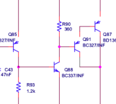
Edit any to-92 Zeltex over BD13x ? (Beta related - and good noise also) ?
Not sure which schematic you refer to?
Basic question :: Is there a possibility to proceed w/o the Farads cells/supercaps ?
Of course. But I find Super Capacitors are to audio what Bacon is cooking. Everything is better with bacon.
The TDA1541 is actually FAIRLY non-fussy on power supplies IF you arrange it right.
For audio, terminate the I/U conversion with the signal current returned to the +5V rail (which limits I/U conversion resistors to 250R and thus audio out to 1V P-P (350mV RMS) and all rails are essentially DC without audio or significant data related currents.
Use the correct RF decoupling to either -15V (preferred) or AGND/DGND (depreciated) and there is little to no AC of any kind in the power supplies.
John Brown used 7805/7905/7915 and it is likely entirely adequate.
But not all analogue stage options return to +5V and not all decoupling reliably resolves all power supply currents to DC.
What I do not understand at that moment is how "regs" contribute to a better sound and a snappier sound related to the TDA11541A voltages inputs (related to the reg toplogy).
It is all down to currents and voltage sensitivity.
Let's first consider a power supply that is Ideal, 0Ohm, DC to light. Zero noise.
No matter what current flows, there is no voltage. Now make the Power supply "non-ideal".
The non zero impedance drops voltages and there is noise.
If we can make the "error" voltage low enough, there is no problem.
In my "Super (Power) Capacitor" design I have 40mOhm from +5V to -15V and a signal current flow of 8mA (2 channels * 4mA) max. which will result in 320uV error voltage across the super capacitor stack. Given 58dB PSRR on -15V the 320uV will become ~400nV in an output signal of 2V. I'm not worried. Noise will end up a tiny fraction of "feck all"
Let's replace it with TL431 without "AC/Noise improvement" capacitors, we now get 8uV/V noise and 60mOhm/V impedance, or 160uV noise and 1.2 Ohm from +5V to -15V. Still very predictable, but a lot more noise and impedance (fixable to a degree of course) and more stuff we do not want getting into our output.
It is important to be clear what specific qualities are needed from the power supply in a specific circuit and to design to deliver these. A truly "universal" power supply is an illusion, it will always way overbuilt for any single application and usually still perform worse than an optimum design.
Follower emitter serie regs works good to me with the TDA1541A. I read everywhere shunt regs were best though ?
Shunts and current sources have the advantage that current loops are clearly defined. Current only goes where we want and there is never any appreciable signal current that escapes into the wider power supply and circuit, the way it happens for series reulators.
When I see those complex charged regs, I am suspisciious ! But I eally having no clue about tech, well here.
Me too, it usually means a lack of requirements analysis and an attempt at a "universally good" circuit.
So, we all agrred the PS and regs topology matter... most !
Least? They need to be matched to the rest.
Okay we do need flat, very low impedance, to ..... what?
Several octaves below 20Hz (say 4Hz - it is what I use as minimum) and depending on details and including local decoupling > 50MHz.
So let's say 4Hz - 50MHz at << 100mOhm across the whole range.
Is it the ended capacitor that has the last word, as far we given it the input good parameters ?
It depends on the exact PSU design. If possible, this is my preference.
Zetex over BD13x ? (Beta/noise floor good couple ? To 92???)
Not really, in the "power" positions we need mainly speed and power handling.
Thor
I set to compare some recent IVs. Common chrs are
If you ask me, any of these are "good enough" relative to the TDA1541 own stuff.
If following with a tube stage with gain, I would return Iout to +5V and make for more simple power supplies, as we do not. see 8mA P-P current.
Thor
Could yoy please guys for the didactic or not, but at least pedagic , why the sunt 'stabilizer" is prefered, at least for daxc ics' ?
Shunt regulators are "deep class A", they must have a standing current that is greater than the worst case maximum signal circuit quiescent + signal current. A graphic and extreme illustration of this principle (source Sound Practices Summer 1993):
This is a "Single Ended" Tube amplifier with 211 output tubes, operating at 1250V/60mA for the output tube.
A second 211 Tube is used to act as shunt regulator for the output tube, a 120mA current source from a 1,400V Supply (scary stuff if you ask me, extremely scary) supplies the circuit.
The 120mA from the CCS can go either into the "signal" tube or the "ballast" tube, the current flow from 1,400V is always 120mA, it never varies.
Essentially we always know exactly where every current flows. Because we have so much current in our shunt element, we can usually make a very "fast" (wideband) circuit with low impedance by the inherently necessary "brute force".
The difference's with a series type regulator should be obvious.
Thor
No it was only brief compare sheet. constant current source is obvious a factor 2 are better. One with BJT and 2 x 1200uF at base. And other with JFET. Actually JFET is winer because of kust one passive R in the ccs circuit. BJT ccs ia also good BUT deserves more bigger elements around.If you ask me, any of these are "good enough" relative to the TDA1541 own stuff.
If following with a tube stage with gain, I would return Iout to +5V and make for more simple power supplies, as we do not. see 8mA P-P current.
And when we take a look at the harmonic content previous IV circuit has more "friendly" harmonics order in the 5th to 7th H, becayse te dacs in general has the same, a bit higher Hs just the same...
,
For my needs "-" concept as CFP NPN is better because of the one big block coupling C going out of the schematic,
and tube can be directly coupled to negative grid bias.
.
I emulate many positive branch IVs all of them are distorting vhen values of Riv are "smaller".
BUT 👽
One, same simplicity positive oriented Riv circuit, is very good and it is sort of "memory cancelation" concept BJT-FET.
Very good I will ost that 🙁
.
Thanks
I made some research on Shunt-end-to-DAC module. Find some optimized solution. It is about components around TL431. just few passive elements are added.
.
And with that it could be possible on board to: populate, not to populate, bypassed, change the values, to adopt to specific need.
.
They are closely related to output impedance of whole circuit, and less with the hum and noise attenuation. I check with avaiable PSpice models. But I am not very satisfied with the models because I read it and i have notion that they are somehow oversimplified and insufficient? The Diodes model for ZT431 (smd) is good, almost the same is from PSpice lib for TI version. One more model is around from Eugen Dvorskin, (the tests made by Chris Basso. unfortunately the test PDF are somehow unavailable... 🙁 No one model emulate real circuit inside with lot of BJTs...
.
Anyway,
IN essence 2 of RC nets can be added to manage PSRR and Zout. It is correlated. Also one BJT is replaced with Darlingtom type TO-92 BJT, (MPSA77, ZTX705, KSP76 or similar) that improved a Zout more and PSRR. TIP31C in current limiting part and BD244C in shunt part (TO-220) are giving the smallest Zout values. Of course that You can use others but these 2 are super available with standard pin order...
.
I tried with very low Rdc L at he output BUT the results are degraded in Zout significantly. So I can not recommend usage of L after the Shunt. A very low ESR of C shunt end is a must. I found one, take a look at the sch, probably there is more in the market...
.
I made corrections on the Pre-regulator module too and I wll post complete circuit.
Thanks
.


.
And with that it could be possible on board to: populate, not to populate, bypassed, change the values, to adopt to specific need.
.
They are closely related to output impedance of whole circuit, and less with the hum and noise attenuation. I check with avaiable PSpice models. But I am not very satisfied with the models because I read it and i have notion that they are somehow oversimplified and insufficient? The Diodes model for ZT431 (smd) is good, almost the same is from PSpice lib for TI version. One more model is around from Eugen Dvorskin, (the tests made by Chris Basso. unfortunately the test PDF are somehow unavailable... 🙁 No one model emulate real circuit inside with lot of BJTs...
.
Anyway,
- RED trace is full circuit, optimized for lower Zout of about 0.125 ohms, good PSRR. (0.6 ohm from 100KHz acc.)
- BLUE is with only 100uF from REF to CATHODE, as many of diy-ers doing, Zout is highest 0.6 ohm cca. And less PSRR. (Also has very high peek around 100KHz to 0.040 ohms)
- YELLOW is almost without the needed elements, Zout is the lowest. PSRR is very low. (0.6 ohm from 100KHz acc.)
IN essence 2 of RC nets can be added to manage PSRR and Zout. It is correlated. Also one BJT is replaced with Darlingtom type TO-92 BJT, (MPSA77, ZTX705, KSP76 or similar) that improved a Zout more and PSRR. TIP31C in current limiting part and BD244C in shunt part (TO-220) are giving the smallest Zout values. Of course that You can use others but these 2 are super available with standard pin order...
.
I tried with very low Rdc L at he output BUT the results are degraded in Zout significantly. So I can not recommend usage of L after the Shunt. A very low ESR of C shunt end is a must. I found one, take a look at the sch, probably there is more in the market...
.
I made corrections on the Pre-regulator module too and I wll post complete circuit.
Thanks
.
I will check some few more things and I will post back the final results. Find the internal schematic at the PDF and some parameters for modeling. The circuit has lets say midle number of elements ut stil it is not so complex... A much lighter in number of elements compared to contemporary regulator ICs...
.


.
There already exists a model for that schematic:
https://www.audio-perfection.com/vo...31-model-development-analysis-and-evaluation/
https://www.audio-perfection.com/vo...31-model-development-analysis-and-evaluation/
The function of -5 V is still unclear for me. Thanks for the excellent analysis of the internals.The -5V supply is not so consequential, but if we tap it off the 20V circuit (so two 5V shunt regulators and one 10V shunt regulator) anyway, it is made to the same standards. And yes, -5V decouples for RF to -15V, not AGND.
@ThorstenL ,
Hello, I was layouting a pcb with 74f74SC (soic) for the sync DEM clock from the Bck pin as per your shematic.
I have few questions please : 2 ICs are used because you use both fliflop of each dual fliflop package ? So it is not only Vcc2 that is biased but also Vcc1, as we also use the others the second fliflop, correct ?
? Do the
Is the mainvoltage of the ICs critical ? Should we use low voltage too like the atenuators ? I see the 74F74 can be poxwered from anything from -0.5 to + 7V ?
It could be also supplied by a cell with low noise and low impedance : LiFePo, or alcalin cell, round watch cell 1.2 to 3.3 V ? Should last long ?!
As the 74F74 is NLA and SOIC should be simplier for layouting, any prefered soic todays reference, please ?
Finally, looking at the temp sensor circuitry, what are T10,T15,T18,T19, lso BC327/337 ? Should they be temp coupled with T13/T14 and the top of the TDA1541A by a sorta of standalone radiator with thermal paste ?
I make a compact core PCB (almost done) with the front end logic as per your shematic but w/o output stage or powersupply, as a dev tool to send to you and to Zoran and myself. If wanted by people, with your absolution sold at a democratic fee for readers here. (with option from 4 layers (low printing price) with no crossed currents and with more layers if wanted (but the price are landing on the pcbs fab then).
The core pcb I layouted is with 0805 resistors and caps for the decoupling but can make a version with 1205 casing for yourself if whished and you don't want to mess with pcb drawing... and make it no verroboard after your first tests (for casing)?
If people interrested, I could propose as well for instance on a standalone pcb an hybrid-Mufollower with the ECC88/E188CC/6N23P-EV tube if readers are interrested. I saw some pop-ups recently, but the layouts I saw are... so-so I have found, so I certainly can make something cleaner about osci and compactness with the good BOM about passive parts... The actives parts are well known since populare Moglia's. But there are plenty of other good shematic with tube. It is just because I have a NIB E188CC I touched at a fair price. But I plan more to try as well the BJT circuitry.
Anyway, let me know if some interrest.
thanks
The function of -5 V is still unclear for me. Thanks for the excellent analysis of the internals.
The exact function is also not clear to me.
I suspect it is the "ballast" (tail current CCS) for the differential logic driving the bit switches that need their Base's pulled below zero.
It's also possible it's part of the the other logic.
It clearly has no functional connection to the audio current sink system between AGND and -15V. The only possible use could be as bias coltage that is uncritical.
The main logic is CMD between +5V and DGND.
So the -5V at significant current seems to have no job? Clearly no. But what job nobody knows it seems. Myself included.
Thor
Thanks. My next plan is to measure the currents of +5 V, -5 V, -15 V and AGND, DGND, in various digital input/analog output conditions, namely at digital zero (i.e. -4 mA), digital half scale (=analog zero i.e. -2 mA) and digital full scale (=0 mA).
I have few questions please : 2 ICs are used because you use both fliflop of each dual fliflop package ?
I wanted to be able to divide up to 512 X FS without pushing ratings, I wanted to be dble to use the IC for re-clocking if I decided I needed it, I wanted DIP IC's and I wanted to buy a single part number.
So I settled on 74XX74 as this gives flexibility and realistically on 74F/AS and 74AC/ACT apply.
I have my reasons for avoiding AC/ACT logic.
So it is not only Vcc2 that is biased but also Vcc1, as we also use the others the second fliflop, correct ?
No, only 2pcs 74F74 are used, each is dual flip flop. They are set up as cascaded divide by 2 chain, so each flip-flop divides the frequency on CK by a factor of 2 at the Q. Do it 4 times, divide by 16.
As long as BCK is 64 X WCK (which it is for standard 24/32 Bit I2S), the divided clock must be 4 X WCK.
We have a diffential (well almost) output from the last flip flop, so we connect Tubee's circuit to drive the TDA1541 DEM Oscillator into phaselock to this clock.
Is the mainvoltage of the ICs critical ?
74F logic is specified for 4.5V...5.5V.
Should we use low voltage too like the atenuators ?
Of course not.
I see the 74F74 can be poxwered from anything from -0.5 to + 7V ?
Where do you see that? No, it cannot.
It could be also supplied by a cell with low noise and low impedance : LiFePo, or alcalin cell, round watch cell 1.2 to 3.3 V ? Should last long ?!
Each 74F74 draws around 26mA static current. Plus the input/output currents.
As the 74F74 is NLA and SOIC should be simplier for layouting, any prefered soic todays reference, please ?
If I was designing to make a PCB, I would use PECL logic for interfacing to TDA1541.
That is MC100EP52 as reclocker and MC100EPT20 as LVTTL to PECL translator.
These only add around around 2-3pS jitter to the MCK applied to the level translator.
If we include a IIS2SIM conversion circuit in 74AUP/AUC logic the DEM clock division logically also resides there and our ECL circuit uses 1 pc MC100EP52 to reclock the divided BCK.
Finally, looking at the temp sensor circuitry, what are T10,T15,T18,T19, lso BC327/337 ?
They form a Baxandall super pair, which acts as buffer to give low DC/AC impedance to the actual sensor. So to speak an emitter follower with 0V Vbe that is not subject to thermal drift.
Should they be temp coupled with T13/T14 and the top of the TDA1541A by a sorta of standalone radiator with thermal paste ?
No. Explicitly not.
T10/15 need to be closely thermally coupled with each other.
If I were making a PCB groundup, I'd use dual transistors from the BC8XX dual range in SOT-23-6. They come in dual N, dual P and N/P.
So a dual N under the TDA1541, N/P for T10/15 and Dual P for the load.
I make a compact core PCB (almost done) with the front end logic as per your shematic but w/o output stage or powersupply, as a dev tool to send to you and to Zoran and myself. If wanted by people, with your absolution sold at a democratic fee for readers here.
Yeah, this is all open sauce, what I am doing here.
The core pcb I layouted is with 0805 resistors and caps for the decoupling
Hard to get C0G/NP0 in large values in that format. I also prefer to specify MELF resistors, the standard ones are appx. 1206 format.
If people interrested, I could propose as well for instance on a standalone pcb an hybrid-Mufollower with the ECC88/E188CC/6N23P-EV tube if readers are interrested.
I would suggest 6N3/5670 or even better 6J1/6AK5 instead. Hybrid Mu... Hmmm. Make it a real one please.
6N6/6N30/5687WB (pins are a LITTLE different!) with E-822 (8.2mA) CRD or whatever is desired as current in the cathode as upper part, extra MOSFET CCS to pull more current out of the cathode.
Then our signal tube below.
Maybe 4 sockets for the signal tube(s), 2 x 7pin for 6AK5, 1 x 9 pin for 5670 and 1 x 9 pin for ECC88 style tubes. Connect grids dnd snodes together, separate cathode resistors to get bias "just so".
And one more 9 pin socket for 6N30/5687 with a switch to select.
We could add a set of small piggyback I/U conversion PCB's with three options:
Resistor I/U conversion with bjt current conveyor to +5V
Resistor I/U conversion with bjt current conveyor to -15V
Resistor I/U conversion with BJT low noise 2mA offset CCS and resistor between AoL/R and AGND.
I will send an E-Mail later today (Monday) to everyone who I know is working on a PCB, so we can pool efforts. Anyone who has been beavering away in lucubrations on the same job, but hasn't told anyone, please PM me so I can bring you in.
Thor
I have a couple of SN74S74N from 30-40 years ago, I suppose they are fast Schottky flip-flops. One of them works as a reclocker im my CD player. I read somewhere the Potato Semiconductor 74G74 is super fast 😉
I have a couple of SN74S74N from 30-40 years ago, I suppose they are fast Schottky flip-flops.
They are. The "S" stands for SLOW.
Semiconductor 74G74 is super fast
Speed as such is not the issue.
But I don't want to use a 74HC74 which does not guarantee use at 25MHz under most listed conditions to divide a BCK that can reach 24.576MHz. Its a bit too close.
And in DIP cases 74HC(T), 74F and 74AC is pretty much the only game.
Thor
- Home
- Source & Line
- Digital Line Level
- Building the ultimate NOS DAC using TDA1541A