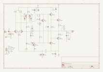
I've taken the liberty to redraw the schematic and to correct the known errors.

Considering the supply voltage, there should be some 1.4 mA flowing through R2. Each of the input differential pair transistors then runs at about 700 uA, giving some 1.05 V of voltage drop across R6 and R7 (neglecting the effect of several base currents).
Subtract the emitter-base voltages of Q3 and Q4 and you will roughly have 0.4 V across R11. Hence, Q3 and Q4 will be biased at about 2 mA each.
A nice feature is that Q3 and Q4 can actually be driven a bit into class-AB thanks to their small tail resistor. When the input stage is driven into clipping, you get 2.1 V across R6 and nothing across R7 or the other way around. The voltage across R11 will then be around 1.4 V, meaning that the second stage can deliver 14 mA peak despite its 2 mA quiescent current - although the distortion will not be low in that regime. For negative currents, R8 limits it to less than 8 mA.
If R6 and R7 were connected to the emitters of Q3 and Q4, the bias current of Q3 and Q4 would be much larger, but also quite unpredictable. It would be the hFE of Q3 or Q4, which spreads all over the place with process and temperature, times the collector current of Q1/Q2 minus the emitter-base voltage of Q3/Q4 divided by R6 or R7.

I would strongly advise you to use a dim bulb tester and not to connect any loudspeakers when you try the changes Hans proposes until you know whether the amplifier is stable.
Iv'e got Q3 and Q4 labled incorrect on the trace side of the pic... Correct pic shown...Here are some pics... I may remove components to reveil the values and then take some pics... Man it's cold in my garage!!! Ugh...
Thanks again you all for having a look, I realize your expertise on this stuff and it makes for a good learning experience for me!!!
Attachments
Wow... Thats a lot of figuring that you did! I will try this on one channel and test it.I've taken the liberty to redraw the schematic and to correct the known errors.
View attachment 1261064
Considering the supply voltage, there should be some 1.4 mA flowing through R2. Each of the input differential pair transistors then runs at about 700 uA, giving some 1.05 V of voltage drop across R6 and R7 (neglecting the effect of several base currents).
Subtract the emitter-base voltages of Q3 and Q4 and you will roughly have 0.4 V across R11. Hence, Q3 and Q4 will be biased at about 2 mA each.
A nice feature is that Q3 and Q4 can actually be driven a bit into class-AB thanks to their small tail resistor. When the input stage is driven into clipping, you get 2.1 V across R6 and nothing across R7 or the other way around. The voltage across R11 will then be around 1.4 V, meaning that the second stage can deliver 14 mA peak despite its 2 mA quiescent current - although the distortion will not be low in that regime. For negative currents, R8 limits it to less than 8 mA.
If R6 and R7 were connected to the emitters of Q3 and Q4, the bias current of Q3 and Q4 would be much larger, but also quite unpredictable. It would be the hFE of Q3 or Q4, which spreads all over the place with process and temperature, times the collector current of Q1/Q2 minus the emitter-base voltage of Q3/Q4 divided by R6 or R7.
Thanks
Scott
The voltage at the juction of R8 and the collector of Q3 is -15.22. Thats with the pos lead on the resistor and the neg lead on power 0 or ground.Apart from the interchanged collectors, everything is o.k.
The only thing I wonder is the 8K2 value of R8, maybe the OP should check this one.
Hans
They are indeed 8.2k resistors, just measured them.
Attachments
Wow... Thats a lot of figuring that you did! I will try this on one channel and test it.
Thanks
Scott
There is nothing to try, as I didn't change anything. I've only corrected and redrawn the schematic of what you already have.
Yes, I see my goof's on the schemi... Getting to old I guess...
So this is it. So how to reduce the offset? Do I change R1 to 12k?
I see my goof's on the schemi... OOOPPPSSS.... Getting too old.I've taken the liberty to redraw the schematic and to correct the known errors.
View attachment 1261064
Considering the supply voltage, there should be some 1.4 mA flowing through R2. Each of the input differential pair transistors then runs at about 700 uA, giving some 1.05 V of voltage drop across R6 and R7 (neglecting the effect of several base currents).
Subtract the emitter-base voltages of Q3 and Q4 and you will roughly have 0.4 V across R11. Hence, Q3 and Q4 will be biased at about 2 mA each.
A nice feature is that Q3 and Q4 can actually be driven a bit into class-AB thanks to their small tail resistor. When the input stage is driven into clipping, you get 2.1 V across R6 and nothing across R7 or the other way around. The voltage across R11 will then be around 1.4 V, meaning that the second stage can deliver 14 mA peak despite its 2 mA quiescent current - although the distortion will not be low in that regime. For negative currents, R8 limits it to less than 8 mA.
If R6 and R7 were connected to the emitters of Q3 and Q4, the bias current of Q3 and Q4 would be much larger, but also quite unpredictable. It would be the hFE of Q3 or Q4, which spreads all over the place with process and temperature, times the collector current of Q1/Q2 minus the emitter-base voltage of Q3/Q4 divided by R6 or R7.
So this is it. So how to reduce the offset? Do I change R1 to 12k?
Yes. If the equipment that drives the input can handle a 12 kohm load, which it probably can, reducing R1 to 12 kohm would be the simplest solution. Also change C1 to 10 uF if you want to keep the low-frequency/subsonic response of the amplifier as is.
When the voltage on R8 is -15.22 Volt, then Marcel is right that R6 and R7 are directly connected to C10.The voltage at the juction of R8 and the collector of Q3 is -15.22. Thats with the pos lead on the resistor and the neg lead on power 0 or ground.
They are indeed 8.2k resistors, just measured them.
I wonder why R8 was made 0.5 watt with only 2mA flowing.
But on the other hand, driving the output stage with this VAS current is a bit low to my taste.
At 28V output, an 8R load will draw 3.5Amp.
Taking a conservative hfe for the output of 1000, this asks for 3.5 mA drive current.
This is just available, but is too marginal IMO.
And 4R would not be within reach.
So, the values of R6 and R7 could be increased to increase the VAS current.
So there are several options to address the offset voltage:
1) attach a Mohm resistor to C10 to supply the exact current to Q1 to get the output voltage at ca zero volt
2) change the 47k input resistor to 12K.
3) change Q1 and Q2 to MPSA14’s and remove the two caps around Q3 and Q4.
I would personally advise to increase the current through Q3 and Q4 to 4mA.
Hans
Perfect, easiest option. Will post results. You all are fricken awesome!! You have know idea!!Yes. If the equipment that drives the input can handle a 12 kohm load, which it probably can, reducing R1 to 12 kohm would be the simplest solution. Also change C1 to 10 uF if you want to keep the low-frequency/subsonic response of the amplifier as is.
Thanks much.
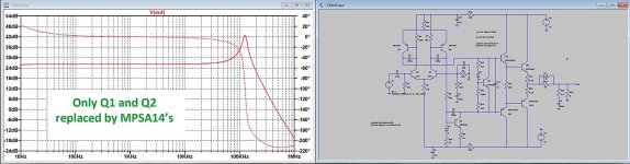
Just for fun, I have simulated the situation with MPSA14's , but now with R6 and R7 connected to C10, as it should have been in the first place.
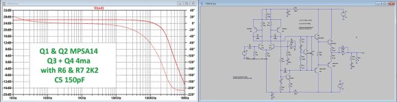
First image shows the FR with only Q1 and Q2 changed into MPSA14's.
Second image shows R6 and R7 changed to 2K2 to get a 4mA VAS current.
At the same time C5 has been changed from 22pF to 150pF.
C7 and C8 didn't have to be removed, just because the output filter caused instability without them.
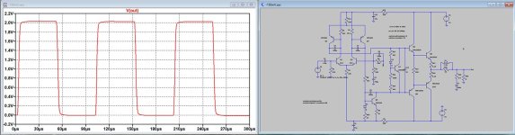
Third image shows a 10 Khz square wave.
All images are with 8R load, and Bias current was 30mA in all cases.
But even with the 4mA setting for Q3 and Q4, output could just get to +/- 22Volt pk-pk with a 20Khz signal.
For a 4R load, maximum output is +/-20Volt pk-pk.
When trying to get +/-24 Volt pk-pk, the required drive current for the output pair became too high, see image 4.
Hans
First image shows the FR with only Q1 and Q2 changed into MPSA14's.
Second image shows R6 and R7 changed to 2K2 to get a 4mA VAS current.
At the same time C5 has been changed from 22pF to 150pF.
C7 and C8 didn't have to be removed, just because the output filter caused instability without them.
Third image shows a 10 Khz square wave.
All images are with 8R load, and Bias current was 30mA in all cases.
But even with the 4mA setting for Q3 and Q4, output could just get to +/- 22Volt pk-pk with a 20Khz signal.
For a 4R load, maximum output is +/-20Volt pk-pk.
When trying to get +/-24 Volt pk-pk, the required drive current for the output pair became too high, see image 4.
Hans
Attachments

Perfect, easiest option. Will post results. You all are fricken awesome!! You have know idea!!
Thanks much.
Attachments
Hans, Does changing Q1 and Q2 to MPSA14's make the amp cleaner or more efficient?
You think I should do the R1 to 12k and C1 to 10u first and see if that change reduces the offset?
Scott
You think I should do the R1 to 12k and C1 to 10u first and see if that change reduces the offset?
Scott
I wonder why R8 was made 0.5 watt with only 2mA flowing.
2 mA is only the quiescent current, the designers probably wanted to keep the resistor alive during prolonged clipping. Even then, 0.5 W is conservative; the momentary power dissipation during clipping to the negative rail is about 0.5 W, but during positive clipping, it should be close to 0.
Hans, Does changing Q1 and Q2 to MPSA14's make the amp cleaner or more efficient?
It should get noisier, but probably not to such an extent that you would notice it. It might also affect stability.
Changing R1 to 12K will drop the Offset without a doubt, when your preamp can handle this, there is nothing against.Hans, Does changing Q1 and Q2 to MPSA14's make the amp cleaner or more efficient?
You think I should do the R1 to 12k and C1 to 10u first and see if that change reduces the offset?
Scott
Using MPSA14’s won’t change the efficiency.
The only thing that’s a bit worrying on this amp is the bad way the clipping occurs.
Hans
- Home
- Amplifiers
- Solid State
- 1988 Amp with 0.150 vDC offset (150mV)