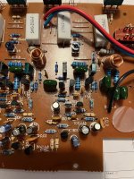
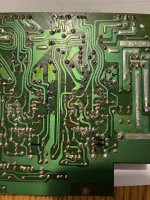
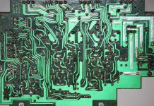
Will do, Will post some tommorow. Thanks AllDoubtfull, never seen that the last 40 odd years. Post a picture of the pcb, top & btm sides.
Ehmm... typo and/or assumption?
edit: R6&R7 are not connected as in #1, it's impossbile. It's hardshortening the loop gain.
Here are some pics... I may remove components to reveil the values and then take some pics... Man it's cold in my garage!!! Ugh...
Thanks again you all for having a look, I realize your expertise on this stuff and it makes for a good learning experience for me!!!
Thanks again you all for having a look, I realize your expertise on this stuff and it makes for a good learning experience for me!!!
Attachments

Last edited:
That amp does not have a LTP degeneration, a current mirror, Baker clamp(s), a Darlington VAS, a VAS CCS. So, I dunno if I would call it "Blameless". R11, R12 at 220 are asking for shoot through current. 100 Ohms would be marginal, and I would go 47 Ohms. Possibly also not shown is L-R output isolation network to prevent stability problems caused by the speaker cable... A CFP output is not my favorite because it does not cross-couple easily, one thing your old amp did well. You may also consider 2-pole compensation. Simulation is recommended.Steveu, I'm considering it... Maybe with https://sound-au.com/project3a.htm
Darlington VAS? No, emitter follower is the Blameless VAS - you avoid non-linearity from the Miller capacitance that way as the first transistor collector is at ac ground.
If in the schematic of post #1, the upper sides of R6 and R7 were connected to the positive side of C10, it would simply be a cascade of two differential pairs with reasonably predictable biasing.
They are.If in the schematic of post #1, the upper sides of R6 and R7 were connected to the positive side of C10...
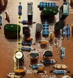
In yellow the plus supply rail.
Attachments

Point is that the collectors of Q3 and Q4 are interchanged in the shown circuit diagram, leading me to a wrong conclusion.
To bring both collectors at the same voltage, 8K2 should indeed be lowered to ca. 3k3, this will prevent Q4 to go into saturation.
At the same time the offset voltage at the output is to blame to R1 and R4 being different, resp 47K and 12K.
You could replace Q1 and Q2 by MPSA14 darlingtons, that will reduce the offset to a few mV.
When doing this, C7 and C8 will have to be removed.
Hans
Point is that the collectors of Q3 and Q4 are interchanged in the shown circuit diagram
You are right about that, it is positive feedback now.
So, in the schematic of post #1, the collectors of Q3 and Q4 have to be swapped and the upper sides of R6 and R7 have to be connected to the positive side of C10.
Connecting R6 and R7 directly to C10, but leaving R11 in place, will lead to almost shutting off Q3 and Q4.
Or did you have in mind to replace R11 by a short ?
If so, that will have no measurable impact.
Hans
Or did you have in mind to replace R11 by a short ?
If so, that will have no measurable impact.
Hans
I hadn't spotted the positive feedback. 🙁
OP said he was working on an existing amp, so how did the posted schematic come to be? What other errors are there? Seems like a trustworthy schematic is a first order need.
OP said he was working on an existing amp, so how did the posted schematic come to be? What other errors are there? Seems like a trustworthy schematic is a first order need.
Apart from the interchanged collectors, everything is o.k.
The only thing I wonder is the 8K2 value of R8, maybe the OP should check this one.
Hans
The only thing I wonder is the 8K2 value of R8, maybe the OP should check this one.
Hans
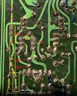
I painstakingly sketched it out with a lighted magnifying lens and multimeter... Ugh... I've checked it a few times to make sure its correct.I hadn't spotted the positive feedback. 🙁
OP said he was working on an existing amp, so how did the posted schematic come to be? What other errors are there? Seems like a trustworthy schematic is a first order need.
If I try this... I have a bunch of NOS MPSA14's, remove C7, C8, Replace Q3,4 with MPSA14's. Do I need to also reduce R8 to about 3.3K?Point is that the collectors of Q3 and Q4 are interchanged in the shown circuit diagram, leading me to a wrong conclusion.
To bring both collectors at the same voltage, 8K2 should indeed be lowered to ca. 3k3, this will prevent Q4 to go into saturation.
At the same time the offset voltage at the output is to blame to R1 and R4 being different, resp 47K and 12K.
You could replace Q1 and Q2 by MPSA14 darlingtons, that will reduce the offset to a few mV.
When doing this, C7 and C8 will have to be removed.
Hans
And check bias...
Scott
No, not Q3 and Q4, but Q1 and Q2 should be replaced by MPSA14’s.
And yes, removde C7 and C8.
I strongly advise you to replace R8 into 3K3.
Hans
And yes, removde C7 and C8.
I strongly advise you to replace R8 into 3K3.
Hans
And remenber to reduce the bias current before you start and to adjust it again after the alterations.
Hans
Hans
- Home
- Amplifiers
- Solid State
- 1988 Amp with 0.150 vDC offset (150mV)