For now, I try to figure out public acceptance of my brute-force approach to audio.So ska, do you want to share you design or only show it off ;-)
Both are f course ok...
//
170dB negative feedback in the modulator, and accurate layout design of the small FIRDAC, that is it.
The DAC is very good, I've never listen to something that sounds better, but I'm not an audio expert and I'm not an independent referee.
Again - if it is a market investigation for a commercial endeavour - you should ask a moderator to move the thread to the commercial sector. You do it by reporting your own post and state your matter.
If it sounds good, it's reasonably priced and can be DIYed - why wouldn't it be accepted. Many examples here - search for e.g. "DAM DAC".
//
If it sounds good, it's reasonably priced and can be DIYed - why wouldn't it be accepted. Many examples here - search for e.g. "DAM DAC".
//

How about galvanic isolation of the spdif/usb inputs, presumably via optocouplers? Toslink has high jitter and is used in consumer audio only, not in high end. multiple switchable inputs is a must have feature for a marketable product, but it can be handled by a dedicated board.TOSLINK is the best way to get rid of ground loops.
That's one way. There is also FIFO buffering which can work well for consumer audio with TOSLINK. The downside is the buffer delay. Also, the more you do to improve a dac, the more you find out what's still wrong with it. Galvanic isolators don't stop radiated EMI/RFI problems. The isolation gap is to short, so you need shielding too. Its one thing after another.
I handle TOSLINK inter-symbol-interference by using low bandwidth PLL. It is implemented in FPGA, because of extremely low frequencies (0.03Hz) it is near impossible to use regular capacitors and resistors.How about galvanic isolation of the spdif/usb inputs, presumably via optocouplers? Toslink has high jitter and is used in consumer audio only, not in high end. multiple switchable inputs is a must have feature for a marketable product, but it can be handled by a dedicated board.
The PLL very slowly adjusts VCXO frequency keeping zero phase shift between system clock and clock, recovered from TOSLINK data stream. Frequency response of the PLL loop filter is of 3-rd order low pass filter with a cutoff 0.03Hz. Thus, the clock purity depends only on VCXO phase noise.
I’m listening music exclusively from the PC computer, using USB to TOSLINK interface based on CM6631A.
The computers are extremely noisy staff. It is very difficult to get rid of digital and SMPS noise, especially if you use a power amplifier with switched power supply from another side. That was the motivation to use only optical connection.
You just plug it in and don’t care. All digital sources sound equally good, even smartphones.
Last edited:
FIFOs for "reclocking" are not used in professional setups as they introduces latency and by principle cannot avoid buffer issues (longer FIFO/latency => later issues).
BT audio is lossy due to low bandwidth capacity. Only the very latest BT codecs are lossless but these are available on very limited selection of devices/transmitters.
Unless an async network protocol is used (Squeezebox, DLNA), standard streaming (just like SPDIF) carries clock with the stream which must be async resampled to the DAC clock.
IMO USB audio async is the easiest protocol of all which allows master clock to be placed with the receiver.
J-Test has nothing to do with SPDIF.
Julian Dunn, the inventor of J-test would differ I suspect. He said 'J-test is an AES3 test signal....'. Since AES3 and S/PDIF are strongly related your claim looks to be on shaky ground.
When J-test was invented AES3 was practically the only standardized interface used for exchange of digital audio so naturally that was its intended use case. But J-test as a test signal has nothing to do with SPDIF. Nor is its use limited to AES3 interfaces only.
From the photo of the board, it appears that a 16-tap FIR is constructed using u21, u19, u15, and u27. In such a configuration, based on my experience and other implementations, I think that even with a perfect power supply, there might be noise, possibly around 10μV. This noise can stem from factors like switching noise in ICs and differences between LtoH and HtoL transitions. Reducing the clock frequency can improve this issue by decreasing the number of transitions, as you mentioned.Thanks George,
High SNR is very difficult thing to achieve, and very questionable for audio. For example my LPF has only 6uVrms noise.
With 1Vrms output it provides me exactly -104dB noise floor. But my power amplifier has standard +24dB of gain.
First-order DSM can decrease the transitions, but less noise-shaping results in poor THD. I guess even PWM might encounter similar constraints. Are there any secrets involved😉, especially considering that ICs like u21 seem to be uncommon 8-pin devices? Achieving a noise level of 6μV with a sixth-order analog filter is normal performance. However, with a 16-tap FIR, the first notch appears around 140kHz. Therefore, it seems unnecessary to deliberately introduce an analog filter, IMO. In my own implementation with a 16-tap FIR, a simple 6dB/octave analog filter is enough.
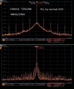
I've also attempted to use an external oscillator with an FPGA to separate the clock from TOSLINK. However, the results were unsuccessful, and I eventually gave up the TOSLINK approach. Even commercial chips claiming top performance yielded a similar performance (pic#1) as cs8416. The recovered clock (24.576MHz) exhibits certain spectral elements and Gaussian-like phase noise. Due to TOSLINK specifications, which allow the clock to only be bursty, and inconsistencies in the optical cable delay, a successful result was impractical. If you have succeeded in recovering the clock without issues, that's fantastic 🙂.I handle TOSLINK inter-symbol-interference by using low bandwidth PLL. It is implemented in FPGA, because of extremely low frequencies (0.03Hz) it is near impossible to use regular capacitors and resistors.
The PLL very slowly adjusts VCXO frequency keeping zero phase shift between system clock and clock, recovered from TOSLINK data stream. Frequency response of the PLL loop filter is of 3-rd order low pass filter with a cutoff 0.03Hz. Thus, the clock purity depends only on VCXO phase noise.
I’m listening music exclusively from the PC computer, using USB to TOSLINK interface based on CM6631A.
The computers are extremely noisy staff. It is very difficult to get rid of digital and SMPS noise, especially if you use a power amplifier with switched power supply from another side. That was the motivation to use only optical connection.
You just plug it in and don’t care. All digital sources sound equally good, even smartphones.
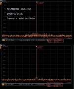
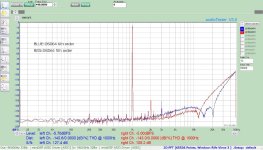
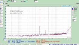
Nevertheless, since optical transmission is crucial, I've employed a simple phase modulation to send data. This also involves an external oscillator combined with an FPGA, achieving performance comparable to the AMANERO (pic#2). For reference, the clock from the Raspberry Pi (pic#3), often considered the worst, does not exhibit Gaussian-like noise. I guess it has no delay inconsistency.
Attachments

CS8416 is from 2002... I would think that this tech has progressed somewhat since? Arn't there better chips?
//
//
The RPi-generated BCLK combines two clock periods (divider M and M+1) to obtain approximate average of the exact required frequency https://www.diyaudio.com/community/threads/avoiding-rpi-master-i2s-fractional-jitter.376583/ .For reference, the clock from the Raspberry Pi (pic#3), often considered the worst, does not exhibit Gaussian-like noise. I guess it has no delay inconsistency.
I assembled 2 versions with 8-tap and 16-tap FIRDAС. The photo is 8-tap version, 16 version is already mounted in some enclosure. I used regular LVC2G74 series flip-flops, I believe Mola-Mola has the same ones.From the photo of the board, it appears that a 16-tap FIR is constructed using u21, u19, u15, and u27. In such a configuration, based on my experience and other implementations, I think that even with a perfect power supply, there might be noise, possibly around 10μV. This noise can stem from factors like switching noise in ICs and differences between LtoH and HtoL transitions. Reducing the clock frequency can improve this issue by decreasing the number of transitions, as you mentioned.
First-order DSM can decrease the transitions, but less noise-shaping results in poor THD. I guess even PWM might encounter similar constraints. Are there any secrets involved😉, especially considering that ICs like u21 seem to be uncommon 8-pin devices? Achieving a noise level of 6μV with a sixth-order analog filter is normal performance. However, with a 16-tap FIR, the first notch appears around 140kHz. Therefore, it seems unnecessary to deliberately introduce an analog filter, IMO. In my own implementation with a 16-tap FIR, a simple 6dB/octave analog filter is enough.
Аll resistors are Bourns 8-res assemblies 0.1% 10k ок 5К, what was found in the drawer, leftovers from previous projects.
The LPF is of very specific design for low distortion and low sensitivity to high frequency noise.
The idea was taken from old Russian patent and modified for more HF tolerance. Nothing similar was found in the textbooks. It was probably over-engineered because of similar performance of 8t and 16t FIRDAC versions.
The noise was sacrificed to linearity and HF tolerance.
The key to proper clock recovery is PLL low bandwidth. The loop filter averedges phase error for about 45 seconds with VCXO DAC update rate of 5Hz. To suppress SPI transmission noise, the DAC is updated only if necessary. Sometimes it stays the same for seconds, because of static error for 3-rd order control loop is 0.
Last edited:
So a bit like....For now, I try to figure out public acceptance of my brute-force approach to audio.
🙂
//
Agreed, and it can result in lower close-in phase noise if using good crystal clocks.IMO USB audio async is the easiest protocol of all which allows master clock to be placed with the receiver.
That said, its not clear what this dac can sell for. The high-sales-volume consumer market is mostly for dacs selling for no more than a few hundred dollars. Even the original Topping D90 was a bit too expensive at around $700.
Moving along into the lower end of the high end commercial market, there are dacs boxes still using dac chips, but with better circuitry surrounding the dac chip, and more bells and whistles.
At around $4.5k or so there are some lower end Holo dacs that are very popular with audiophiles. There are also some R2R type dacs and alow end Chord at closer $1k, but they don't sound very good.
The dac of this thread is of unknown SQ. It may not play DSD from an external source, it doesn't have much or anything in the way bells and whistles, etc. Unless it sounds as good or better than a Holo Spring 3 or similar (which can play external DSD, and has some bells and whistles) this can probably can't sell for more than, oh, maybe $2,400. Divide that by 6 gives 400. That means the complete dac, the manual, the shipping box, case, the power supply, the USB board, TOSLINK cable, factory testing, and whatever else, needs to have an incremental production cost of no more than $400. That's because nobody is going to buy a diy board for $2400 unless it sounds better than a Bruno Putzeys dac.
OTOH, how much could the DAC fetch as a diy product? Well, most people buying dac boards around here are looking for low cost. They may try a cheap discrete resistor dac, but very few will pay for an expensive diy dac board. Also, if you sell diy, you are going to have customers that need technical help and support. A one man operation has to provide that. OTOH, if you are in the high end commercial market, most warranty support, advertising, dealer recruitment, etc., type things will handled by regional distributors. The distributors get maybe a 10% cut of the selling price as their payment for the work they are responsible for. Dealers might get 30% of the selling price. The other 60% goes to the manufacturer. However, if you have distributors and dealers all over the world, you may end up better off by essentially paying other people to do part of the work.
It's quite intriguing. I've come across differential PWM implementations where XQ is created with its unique reference voltage, not simply an inversion of Q. Is your circuit designed in a similar manner? If not, there might be no need to implement separate ICs for Q and XQ.I assembled 2 versions with 8-tap and 16-tap FIRDAС. The photo is 8-tap version, 16 version is already mounted in some enclosure. I used regular LVC2G74 series flip-flops, I believe Mola-Mola has the same ones.
Аll resistors are Bourns 8-res assemblies 0.1% 10k ок 5К, what was found in the drawer, leftovers from previous projects.
The LPF is of very specific design for low distortion and low sensitivity to high frequency noise.
The idea was taken from old Russian patent and modified for more HF tolerance. Nothing similar was found in the textbooks. It was probably over-engineered because of similar performance of 8t and 16t FIRDAC versions.
The noise was sacrificed to linearity and HF tolerance.
The most basic PWM, much like a first-order DSM, tends to have long durations for both high (H) and low (L) states, lacking effective noise shaping and resulting in poor total harmonic distortion (THD). When applying deep feedback, how does the output waveform change for PWM? I would expect shorter durations for H and L, causing quantization noise to shift towards higher frequencies.
The attached images are the digital domain characteristics of the fifth and sixth-order 1-bit DSM with 64OSR (pic#1) and 128OSR (pic#2). For an eighth-order PWM, I'm curious about the frequency at which quantization noise starts to rise. If you have FFT data, that would be appreciated 🙂.
Attachments
Hi xx3stksm,
This is the performance of the entire digital path of the DAC. I mean 48K input up-sampled and filtered to 768x.
The output was taken from Verilog simulator. Additional moving average of 16 consequent data samples applied(FIRDAC model).
Input level was 0dB, that means about 0.54 modulation depth. FFT length - 2**20.
On the physically measured spectrum, the noise "break wall" is visible from about 100K only, due to very high loop gain of the modulator.
The modulator pushes almost to near 0 all kind of distortions and noise floor modulation.
You can notice even a small fall down above 20kHz, where Digital Filter cuts out a chunk of 24-bit quantization noise.
All you need - to fight only analog domain artefacts.
I don't understand the source of the 2-nd harmonics on you attached pictures, because of digital output of the modulator
is always free from even harmonics. Simply by principal of operation.
- Home
- Source & Line
- Digital Line Level
- Discrete FPGA DAC project