Hi,
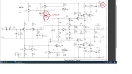
I could really need some help here. As my first serious project, I built this low power complementary feedback amplifier design by Randy Slone. Then I powered it up, with input shorted to ground, everything aperaed to be be ok. Ran it at +/-15 V from my bech power supply. Current draw was like 100 mA per rail or so. I set the bias voltage across the driver transistor to 1,3 V (as suggested). But then powered it up without any input, the zobel-network resistor (R38) literary went up in flames.
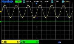
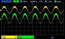
So I guess I hove some serious problems with high frequency oscillations here. Powering up the amp without anything connecting to the input is impossible. However I did run it with a 8 ohm dummy load and with signal from my Wavetek signal generator (output impedance in the 150 ohms range or so?). With the amp powered off, the input signal look clean, but then it's powered on both the input and output signal looks like the got a lot of HF noise, see pics. Also the current draw it's quite excessive, like 1,5 amp er rail for a 8 V peak-to-peak output at 8 ohms load. Also I can hear an hissing noise from the board, kinda like the sound from a cheap switch mode cellphone charger...
The problem should be in the feedback path somehow I guess. Disconnecting the singal ground from the output/star/power-ground put the anp in a stable mode again. Really need some help what do here, of course I already double checked the layout, components values and so on. The design is from Randy Slone*s "The Audiophile's Project Source Book" so I doubt it's a design fault.
I could really need some help here. As my first serious project, I built this low power complementary feedback amplifier design by Randy Slone. Then I powered it up, with input shorted to ground, everything aperaed to be be ok. Ran it at +/-15 V from my bech power supply. Current draw was like 100 mA per rail or so. I set the bias voltage across the driver transistor to 1,3 V (as suggested). But then powered it up without any input, the zobel-network resistor (R38) literary went up in flames.
So I guess I hove some serious problems with high frequency oscillations here. Powering up the amp without anything connecting to the input is impossible. However I did run it with a 8 ohm dummy load and with signal from my Wavetek signal generator (output impedance in the 150 ohms range or so?). With the amp powered off, the input signal look clean, but then it's powered on both the input and output signal looks like the got a lot of HF noise, see pics. Also the current draw it's quite excessive, like 1,5 amp er rail for a 8 V peak-to-peak output at 8 ohms load. Also I can hear an hissing noise from the board, kinda like the sound from a cheap switch mode cellphone charger...
The problem should be in the feedback path somehow I guess. Disconnecting the singal ground from the output/star/power-ground put the anp in a stable mode again. Really need some help what do here, of course I already double checked the layout, components values and so on. The design is from Randy Slone*s "The Audiophile's Project Source Book" so I doubt it's a design fault.
Attachments
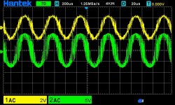
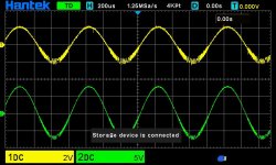
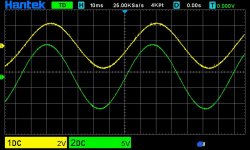
Very interesting. I just did, and it works much better anyway. However it can not be powered wihtou any input (R38 still gets hot and excessive current draw). But it with the signalgenertator it kinda perfomers well, see the pics. Still looks a bit distorted at low signal, but acutally mangaed to get 12 W rsm of it into a 8 ohm load now, see second pic then it starts to clip. Left it like that for some minutes now and it seems stable. Currnet approx 0,8 A per rail.Put a 100pF cap between B and C on the Q14 and Q15.
CFB stage can need this sometimes.
Attachments
Well, that actually seems to do it! after I put the 10 pF cap across R11, the amp seems stable now. Both with and without input. Thanks!
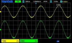
Tried with both 4 and 8 ohms load, about 12W into 8 ohms. and 16W into 4 ohms.
Not sure which sulotion or both that is preferred yet. Both sulotions suggested (100pf across the transistor and 10 pf across R20) worked the best. Maybe I shoul try to change R20 and C10 to?
Strange that it behaves like it does though. Maybe Randy Slne was wrong? Or maybe he somehow intrudiced som capatance into the circuit without knowing it?
Quorious, how did you came up with 1k for R20? There's another design by Slone that has 1k for R20, but that one includes a 2 pole compensating VAS.try change R20 to 1K, C10 to 0.1uF only
Nope, maybe I will tomorrow. This board is quite modified beyond recognition anyway.Have you tried 10 ohm resistors in series with the bases of Q16, Q17, Q18, and Q19?
Put a 100pF cap between B and C on the Q14 and Q15.
CFB stage can need this sometimes.
how do you calculate it so quickly?try change R20 to 1K, C10 to 0.1uF only
this is a real question because I haven't entered the matrix yet and it really takes me a long time to judge the whole schematic.
Well that kinda make the trick. Tried 136 pF (soldered another 68 pF across it) and now it looks much better. Also tried to remove and add some other modifications. The best solution so far;Have you tried increase the compensation cap C8 ?
From 68pF to 100pF or 150pF
- 100 pF across B C at Q14 and Q15
- C8 to 136 pF
Changing R20 does not seem to have any efect at all.
Tried remove 10 pF across R20 and it actually made it a little better without, see the pics. The 100 pf across B C at hte driver transistor seems to be a must have anyway. Strange that Slone did not include this in his design, or are the transistor (2SD649/2SB669) of some fake sort with different characteristics?
Attachments
The circuit looks basically OK, and it should work with little or no modifications; however the devil is in the detail, and layout, components etc. might have large, unexpected effects.
The problem with feedback-related issues (which is almost certainly the case here) is that they depend on the actual components used: whether you use the slow-hand pen and paper method or simulation, you need accurate data about the components you use, and this is not simple: modern versions of the components listed probably have little in common with the originally specified types.
Some cheap fakes might be heavily downgraded, but the tendency for modern substitute from asian origin is to use a process that vastly outperforms the original one regarding Ft, etc.
They comply with the datasheet, because only minimal or typical values are published, but their HF performance can wreak havoc in legacy designs.
A way forward is probably to start with an heavily overcompensated circuit, as has been suggested before, use a 330pF compensation cap or more, possibly with a small series resistor to introduce a zero in the TF, and work incrementally from there, using a squarewave as a stimulus to monitor the ringing, etc.

Hi Bengtssk,
Ive found that supply impendance often reduces stability substantially.
Have you tried connecting more ceramic decoupling caps across from supplies to ground? This will cancel out some more inductance in your supply lines. Supply inductance can cost you lost of gain and phase margin. It might help to use more supply capacitance as close to the output devices as possible (ceramic caps too). I place a ceramic cap at each point where a transistor meets the supply.
Id also try some 22 to 100 pF from the bases of Q15&14 to ground.
I'm also trying to figure out howto get rid of some ringing at clipping. More decoupling doesnt always help but maybe it this case it does since you already use lots of high frequency compensation. Though even more compensation will help for sure.
Cheers and good luck!
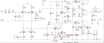
The resistor values are designed for a higher supply voltageTried to change R20 to 1k, no chnge at at all. Listened to the amp, and it sounded ok. But the oscilloscope still shows some HF-"****" that I don't like.
if you run it in +/-15V for testing , you need change below resistors to get a correct current
Attachments
Last edited:
I think it's a typo mistake in the bookQuorious, how did you came up with 1k for R20? There's another design by Slone that has 1k for R20, but that one includes a 2 pole compensating VAS.
if R20 is 100 ohm then the first VAS transistor Q10 current will be more than 6mA, it's not a good idea
Attachments
R20 and many more.
This case 330 , 470 more than enough for beta enhancement
The design is nice and straight forward.
I just dont understand why such a fancy frontend.
To just use TIP31 / 32
Cross conduction will start rather early.
This amp will have high frequency issues even if the board
was textbook perfect.
@patrick101 observations are rather spot on.
If your testing at lower voltages the current sources wont be correct.
Miller compensation C8 being raised to the moon probably helped.
But original value is more than adequate. Raising it will help.
But will never fix the issue no matter how high.
Actual it will kill on time at high frequency, and just make it ring more
like any CFP will do.
But actually fixing ringing and cross conduction of a CFP.
Is in (a) first gain stage, (B) feedback loop.
Degen resistors need to be higher, R5, R6 need to be around 220 to 330 ohm.
Takes care of most the issue. other than as mentioned differential with a mirror
then feeding beta enhancement 2nd stage.. woo fun. current is very specific.
anyways... basically more degen will fix the first stage.
Then feedback loop. R11 needs capacitor tied across it.
12k low value so capacitor can be larger than usual.
68 to 100p will kill the ringing.
High frequency ringing will be on the negative rail.
One post showed ringing on positive rail. So it just leads back to the current
sources. Amplifier likely has high DC offset which is positive.
Once DC offset is corrected then ringing will move to negative rail.
With more degen and feedback loop cap. as mentioned should help.
and/ Or use higher Ft outputs, so cross conduction doesn't start so early
The stability is affected by how you build the schematic too. Grounding in particular.
This circuit wants to oscillate; it's not a very stable design. You'll end up tweaking it until it is stable enough not to catch fire but then it won't sound great. Useful learning experience, though.
This circuit wants to oscillate; it's not a very stable design. You'll end up tweaking it until it is stable enough not to catch fire but then it won't sound great. Useful learning experience, though.
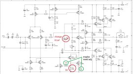
Thanks for all you replies, this has been very helpful. After some testing and more reading I think that now have a working amp. The attached schematic is uppdated with the new values.
Used 330 ohm, what does this resistor do? Changeing the values deos not seem to have any big effect.
- removed the 100 pF caps between C and B at q14 and Q15, because they weren't no longer needed.
- Increased compensating capacitor C8 to 150pF
- R3 to 120 ohm in order to increase the the current for the differential pair to 5,6 mA, this because I changed compensating cap C8 to 150. This values will result in a peak current draw for the VAS of about 1,41 mA (8 ohm, 50khz, 30V). And as a rule of thumb the current for the input differential stage should be 4 times the peak current needed. This is from Randy Slone's (ohter) book "high power amplifier construction manual".
- Change R9 and R10 to 2k7, correct @patrick101 . Also after reading "high power amplifier construction manual" I found that the current through them should be approx half of the current through Q1.
- changed the degen resistors R5 and R5 to 330 ohm. This did the trick I think.
- Used 330 ohm for R20, not sure about, so took a value between the suggested ones.
R20 and many more.
This case 330 , 470 more than enough for beta enhancement
Used 330 ohm, what does this resistor do? Changeing the values deos not seem to have any big effect.
Yes, this is what did the trick I think. After changing R5 R6 to 330, I could remove the caps across B C at Q14, Q15. But please explain how this works,But actually fixing ringing and cross conduction of a CFP.
Is in (a) first gain stage, (B) feedback loop.
Degen resistors need to be higher, R5, R6 need to be around 220 to 330 ohm.
Takes care of most the issue. other than as mentioned differential with a mirror
then feeding beta enhancement 2nd stage.. woo fun. current is very specific.
anyways... basically more degen will fix the first stage.
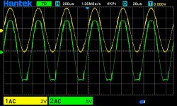
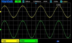
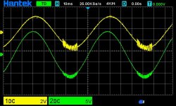
Left it without any cap across it. Then a put a 10 pF cap across it, it actually introduced some HF ringing, see the pics (yellow input signal, green output signal). A bigger cap (68pF or so) did not have any effect though. Found this a little strange, but maybe the 10 pF cap worked like a antenna or something maybe.Then feedback loop. R11 needs capacitor tied across it.
12k low value so capacitor can be larger than usual.
68 to 100p will kill the ringing.
High frequency ringing will be on the negative rail.
One post showed ringing on positive rail. So it just leads back to the current
sources. Amplifier likely has high DC offset which is positive.
Once DC offset is corrected then ringing will move to negative rail.
With more degen and feedback loop cap. as mentioned should help.
fT = gain bandwidth of the output transistors?and/ Or use higher Ft outputs, so cross conduction doesn't start so early
Attachments
- Home
- Amplifiers
- Solid State
- Complementary Feedback design amp oscillating problems