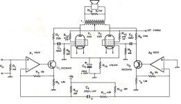
@ jhstewart9 posted this schematic of a Hybrid Transimpedance Tube amp a couple of days ago : https://www.diyaudio.com/community/attachments/transimpedance-amplifier-hybrid-jpg.1158737/
It was presented in Wireless World Mag Oct.1995. I only found a poor, blurred copy of the article and a schematic with all the component values (attached).
So far I understand it the transimpedance part is buried in the sand and not in the vacuum.
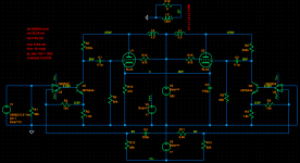
Anyway, over the weekend I put it into LTspice but the result was devastating:
This is not the case in my sim (attached)
Tried 3 different opamp models TL082, OP07, NE5532 to no avail.
Questions:
It was presented in Wireless World Mag Oct.1995. I only found a poor, blurred copy of the article and a schematic with all the component values (attached).
So far I understand it the transimpedance part is buried in the sand and not in the vacuum.
Anyway, over the weekend I put it into LTspice but the result was devastating:
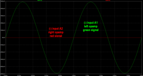
- extremely distorted output even at low levels (claims are 32 W and 0.07% THD at 20 W)
- phase splitting is not working properly (quote from the article: "Phase splitting is produced by coupling inverting inputs A1 and A2 together via R11 and C4. This results in two antiphase equal amplitude signals to drive the output stage." unquote)
This is not the case in my sim (attached)
Tried 3 different opamp models TL082, OP07, NE5532 to no avail.
Questions:
- How is the phase splitting supposed to work ?
- And why does it not work in my sim ?
Attachments

I have no idea why your simulation doesn't work properly. Did you take the usual precautions such as giving the circuit lots of settling time and switching off LTSpice waveform compression?
Judging by the negative-feedback configurations, the solid-state part is a transadmittance amplifier (voltage-to-current converter) and the valve part a transimpedance amplifier (current-to-voltage converter).
Edit: I see that the settling time is only 3 ms while the largest time constants are of the order of 1.4 seconds. You could try a simulation over 10 seconds with waveform compression off and store only the last 4 ms.
Last edited:
You could also reduce the negative supply voltage a bit to give the NPN transistors more headroom, or stare at all waveforms hoping to find a clue. Is an NPN driven into saturation, for example?
right, 1st V/I then I/V ...Edit: I see that the settling time is only 3 ms while the largest time constants are of the order of 1.4 seconds. You could try a simulation over 10 seconds with waveform compression off and store only the last 4 ms.
I never had to do this, but I tried nevertheless : no change ...
OK, so no settling issue. To be honest, I thought it looked too coarse for a settling issue, but you never know.
The only asymmetry in the circuit should be the input signal: the left op-amp gets a sine wave at its input, while the right op-amp doesn't. This is supposed to cause an asymmetry in the waveforms, but only a small one, not the huge asymmetry that you get.
As a sanity check, you could drive the positive inputs of both the left and the right op-amp with equal but opposite signals. If you still get grossly asymmetrical signals, there must be something hidden somewhere that disturbs the symmetry, although I don't see any such thing on the .png of the schematic. Some hidden component imperfection maybe, or something we overlook?
setting Ve- to -15V avoids npn saturation, but that did not change anything with the practically non-existing drive on the right side ...You could also reduce the negative supply voltage a bit to give the NPN transistors more headroom, or stare at all waveforms hoping to find a clue. Is an NPN driven into saturation, for example?
already gone up and down but no clue ...
another mystery I don't understand : I played with the "coupling" resister R11; when I reduce its value, total gain goes up significantly, down at 2.7K gain goes through the roof literally ...
I have no idea if this has anything to do with the problem, but the original circuit appears to use EL84 valves and the simulation model EL34. Perfectly symmetrically, though.
just done that, results in perfect symmetry (I kept the "coupling" network in place);As a sanity check, you could drive the positive inputs of both the left and the right op-amp with equal but opposite signals.
because of the dramatic gain change when I change R11 I am still suspicious about how and whether that phase splitting works ...
been there already, original was EL34 from the paper, the web find is EL84;I have no idea if this has anything to do with the problem, but the original circuit appears to use EL84 valves and the simulation model EL34. Perfectly symmetrically, though.
already tried EL34, EL84, 6GB5 ... only change is in idle current but moderate due to cathode bias.
another mystery I don't understand : I played with the "coupling" resister R11; when I reduce its value, total gain goes up significantly, down at 2.7K gain goes through the roof literally ...
The gain is supposed to be a bit less than inversely proportional to R11, so the gain increase when going from 6.8 kohm to 2.7 kohm is supposed to be a bit less than a factor of 2.5.
The idea is that the voltage between the positive op-amp inputs is copied to their negative inputs by their feedback loops, and hence occurs across R11. The current through R11 then gets amplified 1 + R2/R3 = 1 + R5/R4 times before flowing through the transistors to the valve transimpedance stages.
R3, R4, R12 and R13 spoil it a bit, as they also cause a non-zero gain when the inputs are driven in phase (in common mode). Driving only one side is equivalent to applying both a differential to a common-mode input signal, so having a non-zero common-mode gain means disturbing symmetry when driven on only one side.
Last edited:
Reversre both 220k resistors and 60k resistors. This will allow more voltage swing into the tubes.
Reversre both 220k resistors and 60k resistors. This will allow more voltage swing into the tubes.
Good point. I wondered why the grid leak resistors have such small values. It could very well be that the grid leak resistors are supposed to be 220 kohm and the valve shunt feedback resistors 60 kohm, but they got swapped.
The output signal swing would be too small with 60 kohm shunt feedback. The transistors are biased at about 1.5 mA, so when they are driven all the way to 0 mA, the anodes would only swing up some 90 V.
Also, A2 receives almost no signal. Its inverting input is essentially a short, fed through R11.
All good fortune,
Chris
All good fortune,
Chris
this is exactly what I find, the right opamp gets almost no signal.
so the author's claim :
quote from the article: "Phase splitting is produced by coupling inverting inputs A1 and A2 together via R11 and C4. This results in two antiphase equal amplitude signals to drive the output stage." unquote)
is incorrect ... or there is something missing / error in the original drawing ...
I was wrong, or at the very least incomplete. A1 "drives" R11 with a source impedance of R2 = 10K Ohm. 10K + R11 (=6k8) feed the summing junction, current into the junction is zero'd by current from R5. So signal from A2 is smaller by 10K / 16K8. I'm sorry to have posted in error.
All good fortune,
Chris
All good fortune,
Chris
The transimpedance feedback doesn't work at all for common-mode signals when the primary windings of the transformer are perfect and perfectly coupled. Presumably it doesn't work well when they are imperfectly but still quite strongly coupled.
The op-amp and transistor circuit is not perfectly balanced, which means its output current has a common-mode component. When the valve circuit's feedback doesn't work (well) for common mode, maybe the imbalance at the grids is far worse than in the driving currents.
Could you look at the collector currents of the bipolar transistors and the grid voltages of the valves with a 10 mV peak input signal? I suspect the collector currents are reasonably though not perfectly balanced, and the imbalance at the grids is far worse.

@Chris:
but that's what I get when I "measure" the signals on (-) inputs on A1 and A2.
A1 +/-500mV
A2 +/- 0.1 mV
phase splitting not working at all ... and I can't see anything wrong with my sim, redrawn twice from scratch.
And when I arbitrarily feed A1/A2 with input signals 180 deg out of phase it works flawlessly (with coupling network still in place).
Attachments
The op-amp stuff is modeled on the first half of an instrumentation amplifier, but these rely on a differential input second stage. Too late at night to make any sense, but will be very interested to read y'alls thoughts tomorrow.
XOXO,
Chris
XOXO,
Chris
- Home
- Amplifiers
- Tubes / Valves
- Hybrid Transimpedance Tube Amp Sim