This thread was partly created in response to my query in another "I2S reclock" thread. There are several "I2S reclock" threads here on DIYA, a few 100s of pages long.
For now, I just want the simplest I2S re-clocker possible.
Something similar to:
https://www.diyinhk.com/shop/audio-kits/165-fifo-reclock-jitter-eliminator-for-8-channel-dac.html
IIRC, further tweaking is largely cleaning up pwr rails and decoupling.
Because I put away some projects over a decade ago, I was curious about this veroboard contraption in my "DIYA stuff" drawers.
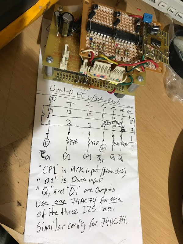
It is a "sandwich" of: Kwack Clock v7 (bottom), I2S reclocker (middle), and Napier /2 (top). All connected togeter somehow (!!) and ultimately used for TDA1541 projects.
The I2S in the photo is based on three 74AC74 logic chips. One for each of the three I2S lines.
If you want to get your feet wet, bare-bones simple, just get three 74AC74 or 74HC74 chips. For starters, you don't even need the veroboard, decoupling caps /ferrites, or even 47R's. You can "fly" three chips with solid wire, like kites, to the pins of the(output I2S) decoder pins and (input I2S) DAC pins. And use any nearby +5vdc power.
That's it.
PS. My notes from the veroboard project say the orig design called for 74HC74. But for some reason, I wound up using 74AC74. Not sure why? Anyone know?
For now, I just want the simplest I2S re-clocker possible.
Something similar to:
https://www.diyinhk.com/shop/audio-kits/165-fifo-reclock-jitter-eliminator-for-8-channel-dac.html
IIRC, further tweaking is largely cleaning up pwr rails and decoupling.
Because I put away some projects over a decade ago, I was curious about this veroboard contraption in my "DIYA stuff" drawers.
It is a "sandwich" of: Kwack Clock v7 (bottom), I2S reclocker (middle), and Napier /2 (top). All connected togeter somehow (!!) and ultimately used for TDA1541 projects.
The I2S in the photo is based on three 74AC74 logic chips. One for each of the three I2S lines.
If you want to get your feet wet, bare-bones simple, just get three 74AC74 or 74HC74 chips. For starters, you don't even need the veroboard, decoupling caps /ferrites, or even 47R's. You can "fly" three chips with solid wire, like kites, to the pins of the(output I2S) decoder pins and (input I2S) DAC pins. And use any nearby +5vdc power.
That's it.
PS. My notes from the veroboard project say the orig design called for 74HC74. But for some reason, I wound up using 74AC74. Not sure why? Anyone know?
Some notes:
Not all I2S lines need reclocking, only the SCK.
If you can find an SN74S74N from some old computer board from the 80's, that is the best. It is not available today.
Use two D-type flip-flops cascaded (in the SCK line) clocked from one common low jitter master clock, in order to prevent metastability.
The DIYaudio team much prefers it when you upload pictures to DIYaudio instead of posting links to some other server.
Some notes:
Not all I2S lines need reclocking, only the SCK.
It depends. That will probably work when the data and word clock are changed at the falling edge of SCK and the ratio of the master clock to SCK is high enough, but the I2S standard does not prescribe that the data and word clock have to be changed on the falling edge.
It also depends on whether the DAC output changes state after a bit clock or a word clock edge. In the latter case, you want a cleaned-up word clock.
Use two D-type flip-flops cascaded (in the SCK line) clocked from one common low jitter master clock, in order to prevent metastability.
It's a valid concern because the master clock to bit clock timing is usually not specified (the I2S standard doesn't even have a master clock), but I doubt that double flip-flops solve it. If the first flip-flop gets metastable and sometimes goes low and in other clock cycles high, you get a 1 master clock cycle peak-peak jitter on the output of the second flip-flop, that is, on the reclocked bit clock. It's better not to reclock at all then.
In some cases MCK is used to generate the I2S signals. E.g. most USB-to-I2S boards have onboard clocks for this purpose. Reclocking with the same MCK downstream should be less prone to metastability as the clocks are more or less synchronous.
You mean MCK --- and not BCK-- correct? In fact, that (MCK, SCK) is the ONLY line I do not re-clock because, for the TDA1541, one must divide by 2 with another logic chip. So I assume the /2 is processing the MCK line enough already.Some notes:
Not all I2S lines need reclocking, only the SCK.
Why that model -- SN74S74N ---and why a vintage chip from the 80s?If you can find an SN74S74N from some old computer board from the 80's, that is the best. It is not available today.
The SN74S74N is still readily avail:
https://www.mouser.com/ProductDetail/Texas-Instruments/SN74S74N?qs=ZA235jQDfboEuDhsajW6Xg==
I mean SCK (sometimes called BCLK or BCK). That is the clock that triggers latching and converting the SD serial data.
74S74 is very fast. There must be a reason why is it still available in spite of considered as vintage.
CD technology is vintage too.
74S74 is very fast. There must be a reason why is it still available in spite of considered as vintage.
CD technology is vintage too.

There have to be integer relations between the master clock and the other clocks for retiming to make sense, but I never see any path delay specifications from the master clock to the other signals. Without knowing the path delay, you can't calculate whether set-up and hold times are met. You can at best use a fast flip-flop and keep your fingers crossed, or try to measure the delay yourself.In some cases MCK is used to generate the I2S signals. E.g. most USB-to-I2S boards have onboard clocks for this purpose. Reclocking with the same MCK downstream should be less prone to metastability as the clocks are more or less synchronous.
If you have them handy, and can measure and show your results (old vs new), that'd be intriguing 😉I have never even attempted to measure it, but I wouldn't be surprised if those old chips produced smaller 1/f sidebands around the clock signals. The tiny MOSFETs used in more modern digital ICs are known for their large 1/f noise.
I do have some new-old-stock logic chips from early 90's. Maybe I'll have closer look myself.
I can't measure it with the equipment I have at home (and the equipment I have access to at work is meant for work).
74LVC1G79 should be fast enough but I don't have suitable equipment to measure the delay.You can at best use a fast flip-flop and keep your fingers crossed, or try to measure the delay yourself.
Keeping in mind the SIMPLE theme of this thread, what would be simple, modern solution for I2S re-clocking.
The chip(s) would have to be avail (stocked) from reputable vendor (DK, Mouser, Farnell/Newark).
I used indiv chips for each I2S line. Is this ideal for noise reduction? Not sure. But this might not be ideal for simplicity. Two 14-pin chips might work.
Nothing smaller than SOIC. Can't proto-board those really small guys easily 😉
I meant the delay from the master clock to the other outputs of whatever drives the I2S bus. In principle, you can look at the delays with respect to the rising and falling master clock edges with a fast two-channel scope and try that at two master clock frequencies (512 times 44.1 kHz and 512 times 48 kHz, for example). Hopefully the delay with respect to one of the edges stays constant, that must then be the active master clock edge. Once you know the delay and the active edge, you can look up the required set-up and hold times of your flip-flop and calculate if it fits comfortably in the available time.74LVC1G79 should be fast enough but I don't have suitable equipment to measure the delay.
The simpler approach is just to use a fast flip-flop and to hope that it works, chances are it does.
I used indiv chips for each I2S line. Is this ideal for noise reduction? Not sure.
It certainly reduces common supply and ground impedance and the associated crosstalk, if you decouple the supply pins of each IC well and have a reasonable ground plane. I doubt if it will make much of a difference on a perfboard without ground plane.
For most SDM DACs, only MCLK jitter matters.
For most older DACs, only LRCLK (WCLK) jitter matters.
BCLK and SData are usually not the subject of a jitter problem.
For most older DACs, only LRCLK (WCLK) jitter matters.
BCLK and SData are usually not the subject of a jitter problem.
Tweaking and iterating ... tweaking and iterating a Philips 74HC74 flip-flop. MCK and BCK entering via same method as I posted in the USB Amanero thread:
Haven't measured it yet.....jitter matters.
Still a bit old-fashioned here.
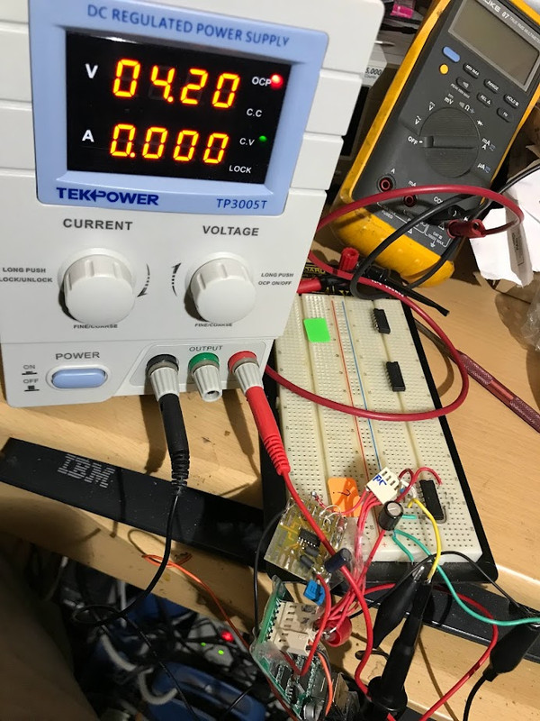
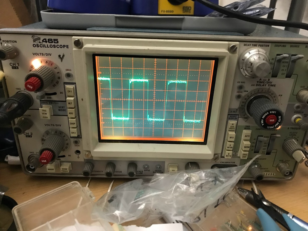
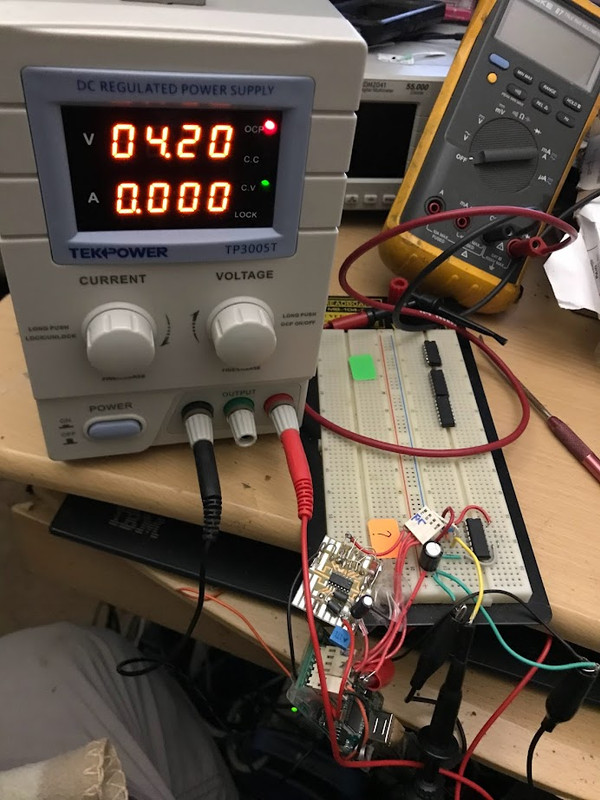
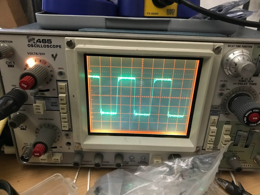
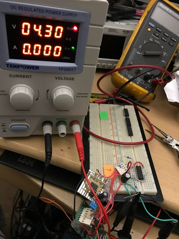
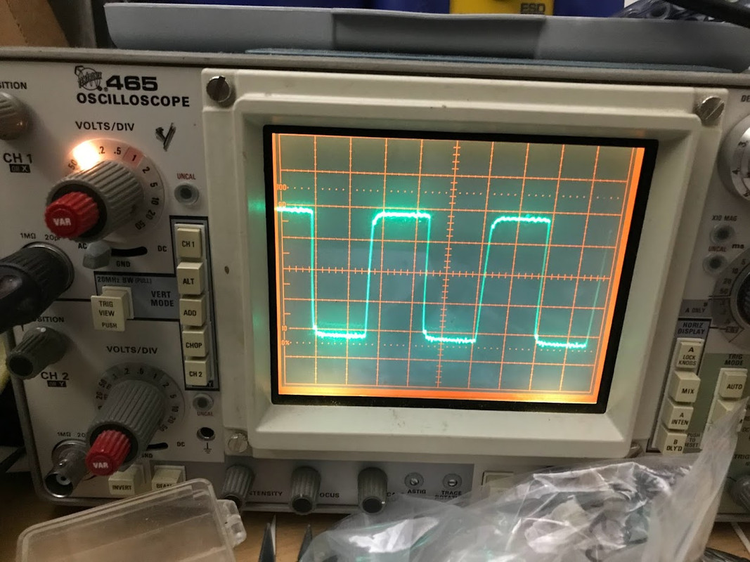
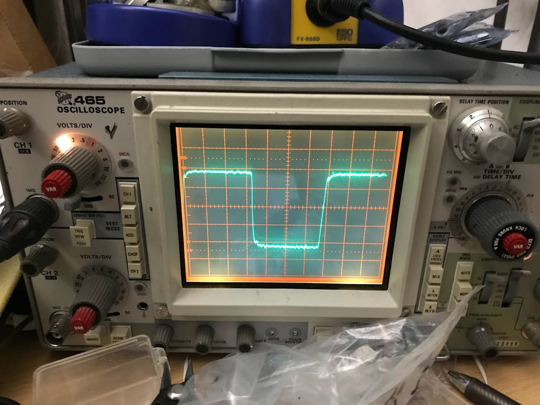
For the breadboard re-clocker (in photos) --- squaring up the BCK waveform was: tweaking power supply voltage (4.2- 4.3vdc seems best); adding R's for in and out digital lines (playing with values. 1 - 100 ohms); combo, values, brands, types (100 uF Pana FM really squared things up ).
Most important: Dreaming spiritual magic.
TDA1541 was mentioned in the OP. It supports various operating modes:
In simultaneous mode the WS triggers the conversion. Resyncing the WS makes sense.
In 2s complement (TWC) and offset binary (OB) mode it is the BCK that triggers the conversion, resynced internally by the SCK sytem clock at pin 4.
The TDA1541A does not have any SCK input. Perhaps it makes more sense to implement an external resync here.
Other DAC chips might work differently.
- Home
- Source & Line
- Digital Line Level
- Re-clocking I2S (simple version)