If you only care about the shape of the clock (which is the maximum you can check with your oscilloscope), you don't need to "re-clock" with D-flop.
You need some kind of buffer.
I prefer 74LVC125 (74LVC1G125, 2G125)
Alex.
You need some kind of buffer.
I prefer 74LVC125 (74LVC1G125, 2G125)
Alex.
Last edited:
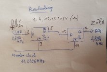
Hi all, I just dusted off an old project of adding an I2S reclocker to my TDA1541A based CD player. I will do reclocking on the BCK line only, the reason I explained earlier in this thread.
And I want do it simple, in the first place, following the philosophy of the topic opener.
Attached is my hand-drawn sketch. For now I will use a Texas Instruments SN74S74N Dual D-type flip-flop, but later I will try some other designed for higher speed.
Since I removed the SAA7220B/P 4x oversampling chip, the BCK is 2.8224 MHz, that is resynced with the 11.2896 MHz low-jitter Master Clock.
It still needs some work but looks promising.
BTW: I read about a "killer" chip, the PO74G74A from Potato Semiconductor. Any ideas how could I get this chip in EU?
Attachments
Makes sense. Anyway, it seems unavailable, and the plain Schottky works well. Alhough I can't measure the effect of reclocking, the first listening experience is good.
I am interested in others' experience with my simple reclocking. It doesn't even need a PCB. I put a 14-pin socket on a perforated board. Apart from this it needs a decoupling electrolytic + ceramic capacitor between pins 7 and 14, and some wires between some pins. My first try was a "deadbug" style 😆 the 74s74 just glued near the tda i2s lines.
No offense intended, its just that we are typically dealing with digital RF signals which have very high frequency components due to pulse edge rise times. Thus, for high quality reclocking, a 4-layer PCB with ground plane should be used. Otherwise jitter/phase-noise are almost certainly going to be worse than they should be. There are various reasons for that, including the need for proper RF EMI/RFI management, controlling transmission line reflections, minimizing ground bounce effects, etc... if reclocking is to be most effective.
that is the way to go - with double serial FF. I experimented and somehow better results are with ALL lines reclockes same way as You did. That will give tha same delay of 2x(1/2) of MCK to the ALL lines not just for BCK line...Hi all, I just dusted off an old project of adding an I2S reclocker to my TDA1541A based CD player. I will do reclocking on the BCK line only, the reason I explained earlier in this thread.
And I want do it simple, in the first place, following the philosophy of the topic opener.
Attached is my hand-drawn sketch. For now I will use a Texas Instruments SN74S74N Dual D-type flip-flop, but later I will try some other designed for higher speed.
Since I removed the SAA7220B/P 4x oversampling chip, the BCK is 2.8224 MHz, that is resynced with the 11.2896 MHz low-jitter Master Clock.
It still needs some work but looks promising.
BTW: I read about a "killer" chip, the PO74G74A from Potato Semiconductor. Any ideas how could I get this chip in EU?
.
Try to put some R as for signal integrity. 1. in the input, 2. between the FFs, 3. at the output. And trim values with a scope to eliminate ringing at the edges. You can round it upon even just below the logic level reached. The values is diferent for each type of FF and from my measurements they are about 47-120 ohms. That will reduce noise and some of the ground bounces. But decoupling the ICs is very important.
.
Just one note the decklocking MCK signal should be as much square. They are usually tend more to sinusoidal shape. Please maeasure. You can apply some sine to square simple circuit with inverters for conditioning MCK line?
.
And from decklocking line of DATA, from -Q of the last FF You can have inverted data for balanced DACs mode? (With "HI" value when no data are present compared to the non/inverted data line where pauses between the words are "LO".)
.
I can report that sound is much more "analog", and less digital harshness, among other less significant improvement, with recklocking all lines with 2x serial FFs
Cheers
.
Last edited:
I would use a single FF maybe this one?BTW: I read about a "killer" chip, the PO74G74A from Potato Semiconductor. Any ideas how could I get this chip in EU?
https://assets.nexperia.com/documents/data-sheet/74LVC1G79.pdf
Yes, the DATA and inverted -DATA is a convenient way to go for balanced. I am not there yet 😏
My MCK is pretty nice, no need any further waveforming. I just had to terminate the end of the coax with 150R to prevent ringing.
For now I use 5V TTL compatible FF, not LV which is for 3.3V system.
My MCK is pretty nice, no need any further waveforming. I just had to terminate the end of the coax with 150R to prevent ringing.
For now I use 5V TTL compatible FF, not LV which is for 3.3V system.
74LVC1G79 works with both 5V and 3.3V (or lower) logic. While not TTL compatible the outputs should work well with any 5V IC such as TDA1541.
You guys are using an active low-capacitance scope probe with spring ground to adjust clock termination resistors? A standard 10x passive probe has enough capacitance to distort a clock waveform somewhat. In that case adjusting the line termination for best clock waveform then removing the probe will leave a somewhat more distorted waveform than was seen on the scope.
If a standard scope probe ground lead is used instead of a spring ground connected to a low impedance ground point very close to where the probe tip is measuring, then the problems are worse due to ground lead inductance ringing with probe capacitance.
If a standard scope probe ground lead is used instead of a spring ground connected to a low impedance ground point very close to where the probe tip is measuring, then the problems are worse due to ground lead inductance ringing with probe capacitance.
Last edited:
Yes this is the best way, thanksYou guys are using an active low-capacitance scope probe with spring ground to adjust clock termination resistors? A standard 10x passive probe has enough capacitance to distort a clock waveform somewhat. In that case adjusting the line termination for best clock waveform then removing the probe will leave a somewhat more distorted waveform than was seen on the scope.
If a standard scope probe ground lead is used instead of a spring ground connected to a low impedance ground point very close to where the probe tip is measuring, then the problems are worse due to ground lead inductance ringing with probe capacitance.
But sometimes it is just "not comfortsble". 🙁
I am trying to take the ground as close as posibile to the pin...
yes74LVC1G79 works with both 5V and 3.3V (or lower) logic. While not TTL compatible the outputs should work well with any 5V IC such as TDA1541.
acc from the datas
thanks
.
And 74LVC1G80 is single FF but with -Q output only.
https://assets.nexperia.com/documents/data-sheet/74LVC1G80.pdf
Maybe it is not bad idea to use single FF with only one output Q or -Q?
Could be separately decoupled?
I dont know...
Thats nice (with good MCK).Yes, the DATA and inverted -DATA is a convenient way to go for balanced. I am not there yet 😏
My MCK is pretty nice, no need any further waveforming. I just had to terminate the end of the coax with 150R to prevent ringing.
For now I use 5V TTL compatible FF, not LV which is for 3.3V system.
Also MCK for clocking should be rising edge, same as BCK.
In some I2S interfaces I measure that MCK is inverted in I2S bus...
(As I am remember that was with some Xmos based USB/I2S interfaces.
Amanero and Savitech based has MCK "in-phase" with BCK.)
So maybe it is not bad idea to measure MCK vs BCK?
Wrong thread?Attached below is some possibly useful info on stabilizing an I/V circuit which has input capacitance to ground.
- Home
- Source & Line
- Digital Line Level
- Re-clocking I2S (simple version)