Sajti
I read it. Thank you very much. In short (extract from 20 pages ) - many people like the amplifier (as I understand, all the assemblies were sold), Takmany is a little better than Vishay rn55, and Silmic is better than Nichikon -)) Did I miss something important?
I read it. Thank you very much. In short (extract from 20 pages ) - many people like the amplifier (as I understand, all the assemblies were sold), Takmany is a little better than Vishay rn55, and Silmic is better than Nichikon -)) Did I miss something important?
Hi,
there was many small changes during the development. Semiconductors was chnaged too, and finally DALE resistors, ELNA Silmic, and Cerafine capacitors are remains.
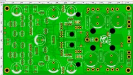
The amplifier was developed for myself, but -as there was some interest-, I sold some pcbs for the diy community.
Sajti
there was many small changes during the development. Semiconductors was chnaged too, and finally DALE resistors, ELNA Silmic, and Cerafine capacitors are remains.
The amplifier was developed for myself, but -as there was some interest-, I sold some pcbs for the diy community.
Sajti
By the way, have you personally compared it to the Apex A40? Can you describe the difference?
No. I never built A40.
Sajti
And you can post it here or to my email even (Locki@ya.ru) throw me the latest version, I want to collect and compare (was it worth soldering so many extra transistors in A40)?
and as I understood from the forum, the SMD option (SMD transistors) did not take root... yes?
and as I understood from the forum, the SMD option (SMD transistors) did not take root... yes?
Hm.. Here's another one... I hope you don't think I'm being impertinent, but if you had sent me a gerber, it would have sped up the process, even though the conversion of the A40 to yours is also quite short, but I would like to hear in the original how you are doing. Thank you in advance.
PS: I can throw my Gerber 40 in response
PS: I can throw my Gerber 40 in response
Attachments
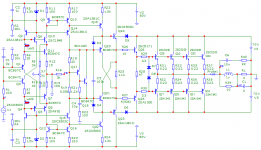
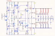
Como vai Sandy, estou fascinado com tudo que você colocou nesse circuito, você montou esse circuito físico???O esquema completo é este:
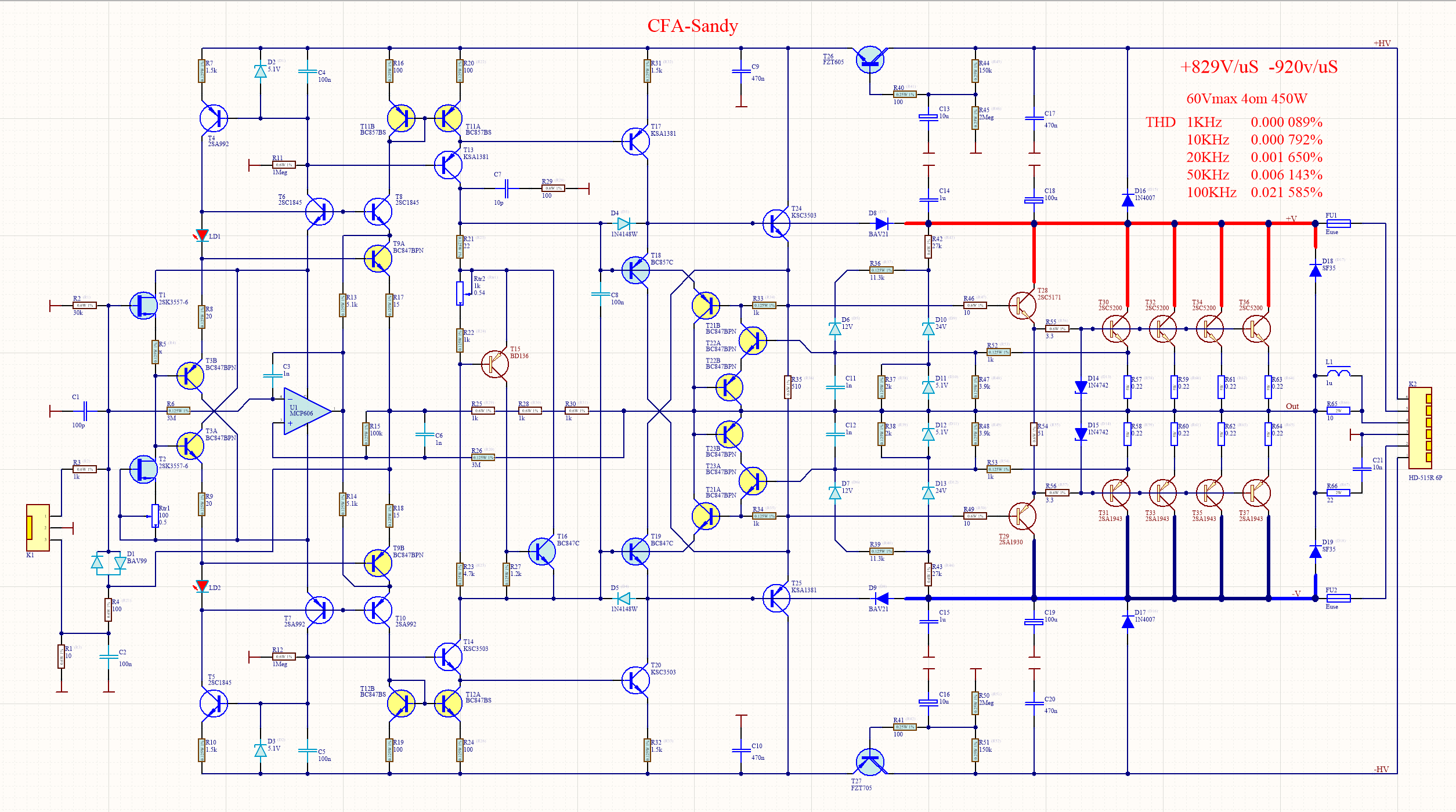
Um CFA servo-livre simplificado foi usado para as simulações
How are Sandy, I'm fascinated with everything you put in this circuit, have you set up this physical circuit ???
English please
dave

duyAudio moderation team

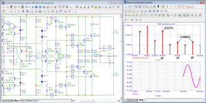
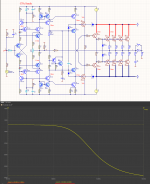
I typed circuit (post 6) in the simulator. Here are the test results.
Attachments
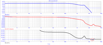
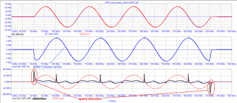
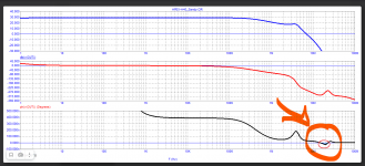
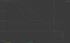
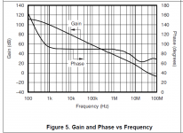
And tell me, please, according to the attached graphs ... You can, if it's not too difficult, explain in more detail what the allocated places mean.
you can also send it to the email: locki@ya.ru or here
you can also send it to the email: locki@ya.ru or here
Attachments
I wonder where is the mistake?
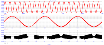
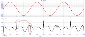
and this is work on active load. And what will happen when working on a reactive load?
and this is work on active load. And what will happen when working on a reactive load?
Attachments


highlighted places indicate a tendency to arousalAnd tell me, please, according to the attached graphs ... You can, if it's not too difficult, explain in more detail what the allocated places mean.
you can also send it to the email: locki@ya.ru or here
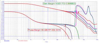
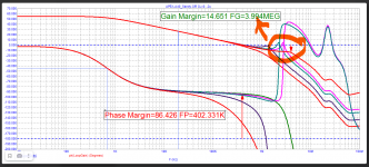
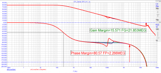
Проверете отново резултата от симулацията.
Фазовият марж е достатъчно голям 78,5 градуса.
Наблюдаваният връх е далеч, където дълбочината на обратната връзка вече е много по-малка от 1.
Increase C5 and decrease R22 and the peak will become smaller, but it doesn't have to be.
Фазовият марж е достатъчно голям 78,5 градуса.
Наблюдаваният връх е далеч, където дълбочината на обратната връзка вече е много по-малка от 1.
Increase C5 and decrease R22 and the peak will become smaller, but it doesn't have to be.
Attachments
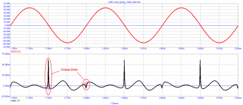
after editing (see pictures):Наблюдаваният връх е далеч, където дълбочината на обратната връзка вече е много по-малка от 1.
Increase C5 and decrease R22 and the peak will become smaller, but it doesn't have to be.
limitations:
1) needs a signal source with a low output impedance (no more than 200 ohms);
2) has a long signal transit time, so increased high-speed distortion is inevitable;
3) the frequency of the first pole is very low, the output impedance is out of phase
Attachments
И тези 3 точки са глупости.
Входният импеданс на усилвателя е равен само на R1+R2 и C1.
А на самия усилвател (вход на T1, T2) вече е 1.149GΩ и капацитет 0.03pF.
Голямата грешка при пресичането на нулата се дължи на малък ток на почивка, през крайните транзистори.
За различните модели е различно, така че го коригирайте към тази схема с вашите модели, за да бъде около 25 mA от всеки краен транзистор.
Това винаги е така при усилвателите от клас AB.
Няма никаква грешка причинена от време на преминаване на сигнала през усилвателя.
Явно нищо не разбираш от тези неща.
Скороста на преимнаване на сигнала през всеки усилвател е равен на скороста на светлината.
Бъркаш закъснение с фазово отместване прочети електротехниката.
Първият полюс не засяга нищо и колкото по-голямо е усилването на усилвателя, толкова по-ниска е честотата на първия полюс.
И да, всички високи честоти вече се въртят на 90 градуса, но това е за усилвателя без обратна връзка.
OPA1612 къде е първият му полюс? \Втората снимка.
Attachments
Голямата ошибка при пресичането на нуле се дължи на малък ток на почивке, през крайните транзистори.
The reason is different - there is no frequency damping at the high-resistance point in the input structure of the cascade. one integrating circuit is not enough.
the first pole determines the linearity of the NFB depth in the audio frequency band. This is more important for the final amplifierbecause it has a reactive load at the output.Първият полюс не засяга нищо и колкото по-голямо е усилването на усилвателя, толкова по-ниска е честотата на първия полюс.
This is done because the op amp needs to be stable over a wide range of gain values used, at least 1 to 20...It's best to correct it by 90 degrees. The power amplifier is designed differently ...И да, всички високи честоти вече се въртят на 90 градуса, но това е за усилвателя без обратна връзка.
OPA1612 къде е първият му полюс? \Втората снимка.
Нищо от това не е вярно.
Теоретичните ви познания са малки.
Можете ли да потвърдите твърденията си с малко теория?
Теоретичните ви познания са малки.
Можете ли да потвърдите твърденията си с малко теория?
- Home
- Amplifiers
- Solid State
- Apex A40 fundamental improvement. (Sandy)