Dear Wes,
Can you kindly post a schematic as built by you ! Did you build it by Point to point or by PCB?
Can you kindly post a schematic as built by you ! Did you build it by Point to point or by PCB?
Hi,
For common understanding and usefulness I suggest we call the components as Blomley did. Otherwise it will be a mess... Too many circuits, simulations and so on and each one has different symbol annotations.
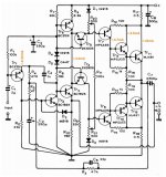
Having said that, my schematic is attached. For me it's easier to order prototype boards instead of working P-to-P style.
Not all of the things that I mentioned in my previous post are reflected in the schematic though. I added them in testing and I'm not done yet. You'll see several capacitors that I use only to specify more footprint sizes. I populate one, or the other, or both accordingly. So, the circuit is correct, but I cannot publish my PCB. It's just a prototype. You shouldn't follow my mods blindly! Just see if they seem reasonable and make sense to you, then take into account the notes in my previous post when you develop your project...
The main point is that the circuit is stable and flexible to adjust if you don't mess with the perfect balance that Blomley designed.
Static currents:

For common understanding and usefulness I suggest we call the components as Blomley did. Otherwise it will be a mess... Too many circuits, simulations and so on and each one has different symbol annotations.
Having said that, my schematic is attached. For me it's easier to order prototype boards instead of working P-to-P style.
Not all of the things that I mentioned in my previous post are reflected in the schematic though. I added them in testing and I'm not done yet. You'll see several capacitors that I use only to specify more footprint sizes. I populate one, or the other, or both accordingly. So, the circuit is correct, but I cannot publish my PCB. It's just a prototype. You shouldn't follow my mods blindly! Just see if they seem reasonable and make sense to you, then take into account the notes in my previous post when you develop your project...
The main point is that the circuit is stable and flexible to adjust if you don't mess with the perfect balance that Blomley designed.
Static currents:
- The input transistor runs at 0.2mA (coming from the output), and at about half the supply voltage.
- There is about 0.8mA to bias the splitter diodes
- The splitter current sources run at about 3-4mA.
- Current through the adjustment circuit depends on the supply voltage, but expect something like 0.4-0.5mA. About the same runs through the first transistor in the triple.
- The drivers in the triple get about 4-5mA
- The output transistors take whatever you set. About 25-30mA is enough.
Attachments
Last edited:

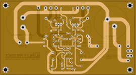
Here’s the new Blomley PCB, as I promised. This is not the final version, some refinements are needed yet. Not single-sided design, but the signal paths are much shorter and clearer in two-sided version. The numbering of the transistors is the same as can be seen in the original Blomley schematic. If anyone finds any errors please let me know.

Attachments
Last edited:
Thank you for sharing your experience.
"1. The gain - 100x is huge by today standards. I dropped it to some 30+ by using R3=3k3, R5=100, C5=82pF."
You're right. However if you increase the feedback, you'll decrease the stability margins as well. In this case GM 4.9dB PM 32° which is very low. (Based on simulation)
"2. Diode OA47 replaced by BAT46 low drop Schottky for obvious reasons of "unobtainium".
The type of didode is crucial here. Some schottkys can increase the distortion at higher level, so experimentation is unavoidable. Perhaps the high distortion experienced during the simulation can be attributed to just this component. An ideal voltage source cannot model real circuit conditions perfectly. If you add a real diode model here you'll get much better result.
Last edited:
I agree. More experiments are needed. I suspect that increasing the feedback capacitor from 33pF to 82pF is not such a good idea. To my understanding this is current feedback circuit. Bandwidth is function of feedback impedance, not gain. So, yes, I have more tests to do. As I said, reactive load tests will show more.
My simulation uses diodes, not a voltage source. The importance of the diodes is to provide a voltage drop somewhere between one and two transistor B-E drops. That depends on the type of the splitter BJTs as well... If we assume about 0.45V for each B-E with such a small current (0.9V for the two transistors), then the two diodes combined should give slightly less than that. With one 1N4148 and one BAT46 I see exactly that. Trimmer adjustments take care of the rest.
Blomley article is very useful. Unfortunately it needs some slow, careful reading and deciphering, because he doesn't show most of the math, just the outcome... I guess it's not very obvious for everyone when he says that the maximum voltage gain is about 30 but can drop to 5, or that there is 1V/1A transimpedance. I guess we should discuss more this stuff to help the circuit understanding. I definitely have parts of the whole thing that still are not 100% clear to me.
1N34A orientation is not correct in the pcb.Here’s the new Blomley PCB, as I promised. This is not the final version, some refinements are needed yet. Not single-sided design, but the signal paths are much shorter and clearer in two-sided version. The numbering of the transistors is the same as can be seen in the original Blomley schematic. If anyone finds any errors please let me know.View attachment 1039074
Thanks for the feedback, I will correct it. And I think I'm going to use BAT46 Schottky instead of a germanium diode1N34A orientation is not correct in the pcb.
Here is the final PCB. The size of the board is 138x76 mm, two-sided. BOM and Sprint Layout file will follow. "PRESENCE" is just a nickname (highlighting the ultimate virtue of the amplifier’s sound), the PCB is based on the original Blomley schematic.

Attachments

Last edited:
Parts for 50V PSU voltage:
Sprint Layout 6 file attached.
- All resistors are 1% 50ppm 0.6W, except the two 0,5 ohms at output which are 3W.
- 2x270uF50V elkos at input
- input capacitor: 2uF16V Nichicon Muse BP or Cornell Dubilier Bipolar electrolityc capacitor
- 33pF and 1nF: at least 100V C0G(NP0) MLCC
- Elkos in PS and output: any low ESR 63V electrolityc that fits on the PCB
- Tr1 - 2N5401
- Tr2 - 2N5551
- Tr3 - 2N5551
- Tr4 - BC556
- Tr5 - BC546
- Tr6 - 2N5401
- Tr7 - 2N5401
- Tr8 - 2N5551
- Tr9 - TTC004B (or 2SC3503C)
- Tr10 - TTA004B (or 2SA1381C)
- Tr11 - NJW8201G
- Tr12 - NJW0302G
- Diodes: 1N916 or 1N4148
- Shottky in splitter circuit: BAT46
- Br1: Bridge Rectifier like this
- F1: standard Fuse holder
Sprint Layout 6 file attached.
Attachments
Last edited:
- Tr11 - NJW8201G
- Tr12 - NJW0302G
Tr11, should this not be NJW0281G?
More notes from my experienceParts for 50V PSU voltage:
- All resistors are 1% 50ppm 0.6W, except the two 0,5 ohms at output which are 3W.
- 2x270uF50V elkos at input
- input capacitor: 2uF16V Nichicon Muse BP or Cornell Dubilier Bipolar electrolityc capacitor
- 33pF and 1nF: at least 100V C0G(NP0) MLCC
- Elkos in PS and output: any low ESR 63V electrolityc that fits on the PCB
- Tr1 - 2N5401
- Tr2 - 2N5551
- Tr3 - 2N5551
- Tr4 - BC556
- Tr5 - BC546
- Tr6 - 2N5401
- Tr7 - 2N5401
- Tr8 - 2N5551
- Tr9 - TTC004B (or 2SC3503C)
- Tr10 - TTA004B (or 2SA1381C)
- Tr11 - NJW8201G
- Tr12 - NJW0302G
- Diodes: 1N916 or 1N4148
- Shottky in splitter circuit: BAT46
- Br1: Bridge Rectifier like this
- F1: standard Fuse holder
Sprint Layout 6 file attached.
Almost everyone in the development laboratory where I worked in 1971 built these (in those days we made printed-circuit designs with adhesive tape and circles on transparent film over hand-penciled designs!).
TR4 and TR5 MUST be FAST SWITCHING transistors. The normal small-signal transistors are not fast enough to "jump the voltage gap" without apparent distortion.
Almost any complimentary PAIR of sufficient voltage (~80v), current (min 6A), frequency (min Ft 100kHz) and gain (10-20) will work as TR11(NPN) and TR12(PNP). Note also that TR 7,8,9,10 also need ~80v capability.
I have driven 4ohm speakers successfully but you have to have sufficient current capability in the output transistors and reduce the output resistors accordingly (R17 and R18).
Peter Blomley specified in the text that he used a 60v regulated output for the 20W amplifier in his article. I have been re-reading his articles for 40+ years and I'm not sure I yet understand everything in it.
Dermot
Blomley used a gold-bonded GERMANIUM diode D5 - OA47 and a silicon diode D4. If you look up the characteristics of the gold-bonded germanium diode at the current (~4.5mA) the voltage is ~1v, hence the need for fast switching transistors to "jump the gap" in TR4 and TR5 as in my post above. I think almost any gold-bonded germanium small-signal diode will work.I agree. More experiments are needed. I suspect that increasing the feedback capacitor from 33pF to 82pF is not such a good idea. To my understanding this is current feedback circuit. Bandwidth is function of feedback impedance, not gain. So, yes, I have more tests to do. As I said, reactive load tests will show more.
My simulation uses diodes, not a voltage source. The importance of the diodes is to provide a voltage drop somewhere between one and two transistor B-E drops. That depends on the type of the splitter BJTs as well... If we assume about 0.45V for each B-E with such a small current (0.9V for the two transistors), then the two diodes combined should give slightly less than that. With one 1N4148 and one BAT46 I see exactly that. Trimmer adjustments take care of the rest.
Blomley article is very useful. Unfortunately it needs some slow, careful reading and deciphering, because he doesn't show most of the math, just the outcome... I guess it's not very obvious for everyone when he says that the maximum voltage gain is about 30 but can drop to 5, or that there is 1V/1A transimpedance. I guess we should discuss more this stuff to help the circuit understanding. I definitely have parts of the whole thing that still are not 100% clear to me.
My OA47 datasheet says Vfmax=0.45V @ 10mA. At 1mA (as in Blomeley amp) Vf=0.3V. From the article is clear that he biases the splitter transistors on the verge of conduction where the linear region has just started. They are not completely off, neither are really on. Two silicon diodes would be too much and both transistors will be pretty much hard on, hence he uses one silicon and one germanium diode....the characteristics of the gold-bonded germanium diode at the current (~4.5mA) the voltage is ~1v, hence the need for fast switching transistors to "jump the gap" in TR4 and TR5 as in my post above. I think almost any gold-bonded germanium small-signal diode will work.
In my prototype I measure exactly 0.86V across the two diodes (Si+Schottky). So, each splitter transistor is at Vbe about half that (0.43V). I'm happy with the result. The BC546B datasheet doesn't show Vbe vs Ic for such a low Vbe but I think they are biased about right. I don't see crossover distortion. Also I measure about 300mVp-p voltage swing at the splitter and the waveform is exactly as he has shown with straight vertical rises/falls. See Fig. 3 in the article.
I understand Blomley voltage gain explanations. We need to take into account re of the input transistor which is about 125 ohms (25mV/200uA). That impedance and R2=3k3 give the max gain of 30 that he talks about. Now if you add to the 125 the R4=470 the gain drops to about 5. All that is good. What I still can't see is the 1A/1V transconductance... Does anyone has a hint on what he meant by that?
For 4 ohms loads we can increase a little the current in the diodes and in the splitter branch. Although Blomley is talking about current gain of 1000 in the triple output. This should be enough drive even for 4 ohms. Maybe I miss something but I don't see how reducing the output resistors will help with driving heavy loads. We can have about a volt more output, but nothing more really. For example if I expect 16V into 4 ohms output, this is 4A current. 2V are lost in the power resistors. If I change them to 0.3ohms, I'll have 1.2V loss. Does 0.8V difference in the clipping voltage really matter? ... considering that idle current and thermal stability will be somewhat degraded.
Last edited:
I was looking for a replacement for the gold-bonded diode so I tried a schottky and a silicon. Small thinking. Two schottkys is good. The essence is that the splitters should use their speed to jump from the positive to the negative (and back) portions of the waveform. This moves the crossover problem to a sufficiently high frequency (many MHz) to really not matter. Just leaving out the diodes doesn't work! Hence the paragraph below.My OA47 datasheet says Vfmax=0.45V @ 10mA. At 1mA (as in Blomeley amp) Vf=0.3V. From the article is clear that he biases the splitter transistors on the verge of conduction where the linear region has just started. They are not completely off, neither are really on. Two silicon diodes would be too much and both transistors will be pretty much hard on, hence he uses one silicon and one germanium diode.
In my prototype I measure exactly 0.86V across the two diodes (Si+Schottky). So, each splitter transistor is at Vbe about half that (0.43V). I'm happy with the result. The BC546B datasheet doesn't show Vbe vs Ic for such a low Vbe but I think they are biased about right. I don't see crossover distortion. Also I measure about 300mVp-p voltage swing at the splitter and the waveform is exactly as he has shown with straight vertical rises/falls. See Fig. 3 in the article.
I understand Blomley voltage gain explanations. We need to take into account re of the input transistor which is about 125 ohms (25mV/200uA). That impedance and R2=3k3 give the max gain of 30 that he talks about. Now if you add to the 125 the R4=470 the gain drops to about 5. All that is good. What I still can't see is the 1A/1V transconductance... Does anyone has a hint on what he meant by that?
For 4 ohms loads we can increase a little the current in the diodes and in the splitter branch. Although Blomley is talking about current gain of 1000 in the triple output. This should be enough drive even for 4 ohms. Maybe I miss something but I don't see how reducing the output resistors will help with driving heavy loads. We can have about a volt more output, but nothing more really. For example if I expect 16V into 4 ohms output, this is 4A current. 2V are lost in the power resistors. If I change them to 0.3ohms, I'll have 1.2V loss. Does 0.8V difference in the clipping voltage really matter? ... considering that idle current and thermal stability will be somewhat degraded.
But please use specifically "fast switching" diodes in the splitters. I think the capacitance of the small-signal transistors is too great to allow a fast-enough rise and fall rate. (I'm not that good with advanced transistor theory...)
[1A/1V transconductance] This refers to the voltage to current converter (Tr2/Tr3) where 1v in gives 1A out (of course a very tiny fraction of that). Effectively the "gain" of a voltage to current converter.
But the output chain from the splitters on has sufficient gain and it's usually the final transistors that are the limitation. You need transistors with sufficient gain at the peak output current - gain drops off quite quickly with current.
Remember that in an amplifier we are not talking about RMS when it comes to clipping but peak (voltage and current of course).
I think a 4-ohm speaker needs just about everything you've got but I haven't really tested that under listening conditions. And the output transistors need lots of "spare" current capability (peak again).
And remember the output transistors need sufficient gain at high current. Gain falls off very quickly at high current.
Final unrelated note. Blomley talks of quasi-complimentary symmetry ad real symmetry almost exchangeably. In those days big PNP transistors were rare. Nowadays genuine matched NPN/PNP pairs are easy. Quasi-complimentary does NOT work as well and has some odd effects like horrible oscillation on turn-off.
Dermot
Member
Joined 2009
Paid Member
And yet quasi-comp output amplifiers have received some accolades for their good sound (NAIM), including some highly popular Chipamps.
I totally agree that in some circuits designed for quasi-complementary output they work very well. And in the Blomley circuit in 1971 they worked better than some of the difficult-to-come-by PNP power transistors. But they came with a really awful switch-off howl (which shows up in the simulation...). Then that was just the price you paid and it was worth it for the presence it gave you.And yet quasi-comp output amplifiers have received some accolades for their good sound (NAIM), including some highly popular Chipamps.
But as I have said before, apparently ANY integrated circuit in any part of the amplifier path somehow introduces intermodulation distortion and the presence disappears.
Dermot
This refers to the voltage to current converter (Tr2/Tr3) where 1v in gives 1A out (of course a very tiny fraction of that). Effectively the "gain" of a voltage to current converter.
The definition of transconductance I understand... Thanks for mentioning Tr2/Tr3 though! I found that Tr3 collector current changes by about 1mA for any 1mV of change on the base of Tr2. What threw me off initially was simulating the schematic with 4 ohms load. If the load is 16 ohm 1V/1A is the ratio. So, mystery solved! ... With 4 ohms it's more like 1V/2A.
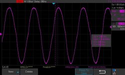
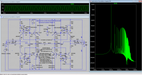
With sine wave of about 300kHz the crossover distortion is well visible (screenshot attached)... Enough for trimmer adjustments just by watching for best response on the scope. In my prototype some 50-60mA give the cleanest sine wave. I was disappointed to see crossover distortion, but then I realized that most amplifiers don't even make it there in frequency response. I'll try other splitter transistors to see if there is any improvement.
2 x Schottky will bias the splitter in class C, to my understanding... with a band in the splitter crossover region where both Tr4/Tr5 are off. I think 1xSi and 1xSchottky is a fine combination.
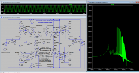
After many trials to balance differently/better the input stage currents and feedback, I can confirm that what Blomley designed is the best overall 🙂 No need to change anything... I only made R9=6k2 because of lower power supply voltage (45V), and the feedback R5=120R to decrease the gain.
For more output power into heavy load either trimmers R20/R21 need to be increased, or R17/R18 decreased. Originally the current gain was set to 500/0.5=1000 by Blomley, but for more output power 1500 might be better. However that will require more idle current and also the thermal stability will suffer. With gain of 1000 and 45V supply I get about 20W/4ohm and this is good for me. I'll do some listening tests soon.
Attachments
Last edited:
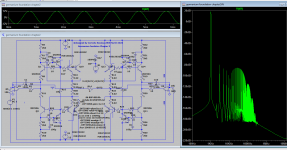
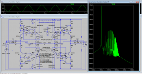
Being inspired by this topic and aided by Molly's simulation I thought of trying some simulations for a new version of germanium amplifer for which I had to use silicon trz models and I think I have better use of the supply voltage in terms of hard clipping behavior with a much simpler up to our date schematic... Enjoy and modify it to your likings if you wish: I made no special stability tests, but have it your way! Soon it will be built too in a lower voltage variation for my germanium trasistors that are barely able to take up 2.5 watts of dissipation ;(
Attachments
-
germaniumfoundationchapter2.asc11.4 KB · Views: 126
-
 germaniumfoundationch2E.png24.6 KB · Views: 209
 -
 germaniumfoundationch2D.png34.3 KB · Views: 194
 -
 germaniumfoundationch2C (2).png34.9 KB · Views: 187
 -
 germaniumfoundationch2B (2).png36 KB · Views: 182
 -
 germaniumfoundationchapter2A.png36.5 KB · Views: 192
- Home
- Amplifiers
- Solid State
- The Blomley Class B amplifier