Decreasing R13 will increase class A stage current (lets name it Iq), formed with Q5 and Q6. This have direct implication on output stage as well, as the bias for output transistors increase as well R11 x Iq and R12 x Iq. Amplifier may no longer operate in class B and, depending on your R13 value, will jump more or less in A/B class.
If R13 is too low, than voltage across R11 and R12 will open Q15 and Q16 completely. These Fairchild are serious transistors, able to surge over 60 Amperes. This is what I think happened in your test, but not at R13=8,35 ohms.
If you reduce R13 you need also to "balance" Vgs on output transistors by reducing R11 and R12 and keep Q15 and Q16 Vgs around 3.1V ~ 3.2V.
I too want a technical opinion!
Are the capacitors going to act as an antenna?
I'm skipping my turn. Hi hi.

With Vishay MAL048 2200uF 63v D18x35.
")
.
Attachments
Last edited:
Hello Tibi,
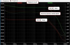
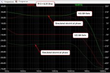
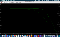
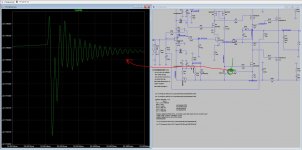
both diagrams are from the same circuit only only R13 is reduced from 10 ohms (original) to 8.35 ohms.
With the original circuit the electrical phase is plausible in both cases with approx. -180°.
In the variant with R13 = 8.35 ohms, the diagrams generated by the simulation are illogical. Here, an electrical phase of +180° is determined for Q6, and -180° for Q5. This shows that the simulation algorithms generate errors.
On the other point:
When enlarging the current damping bridge, R6 = 120 Ohm, i.e. the square root of the enlargement factor - I would now assume.
Attachments
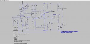
To properly run Q17 simulations, several libraries must be included into project.
These are proprietary, but can be downloaded from:
OPA1641 ->https://www.ti.com/lit/zip/sbom627 unzip and extract OPA1641.LIB
FQA36P15 -> https://www.onsemi.com/pub/collateral/fqa36p15.lib
FQA46N15 -> https://www.onsemi.com/pub/collateral/fqa46n15.lib
FQP3N30 -> onsemi
FQP3P20 -> onsemi
Download these and place in the same directory with Q17 ltspice asc file. Open simulation file with ltspice and include following spice directives:
.inc OPA1641.LIB
.inc fqa36p15.lib
.inc fqa46n15.lib
.inc fqp3n30.lib
.inc fqp3p20.lib
To run transient, uncomment ;.tran 0 200m 100m 10m
Regards,
Tibi
Last edited by a moderator:
Hi!
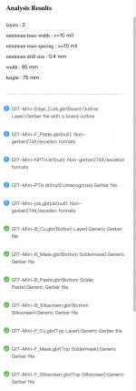
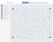
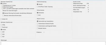
I need help. I uploaded the Q17-Mini Gerber files from my PCB in the jlcpcb system.
The system say that the files have problems. See the screen shot.
Do you know where these errors come from?
Cheers,
Stef.
Gerber files are there: Q17-a-QUAD405-audiophile-approach/Gerber-Q17-Mini.zip at main * stefaweb/Q17-a-QUAD405-audiophile-approach * GitHub
.
Attachments
I too want a technical opinion!
Are the capacitors going to act as an antenna?
I'm skipping my turn. Hi hi.
With Vishay MAL048 2200uF 63v D18x35.
.
Here is my pure personal opinion.
Yes, capacitors can act as an antenna ONLY if you mount incorrectly.
Electrolytic's are made in a metal can and outer foil is always negative. These are less probable to act as antennas.
On some foil and metallized capacitors outer foil is marked on some not. At high signal level is not an issue, but when you deal with very low signal levels, like amplifier input, this can be a major issue for noise and oscillations due antenna effect.
In our case C7 is the capacitor that can change the "note" of amplifier and his outer foil must match with operational output.
Stef, this is a very good point, that must be amended in my PCB too.
Regards,
Tibi
Last edited by a moderator:
Hello Tibi,
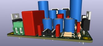
I am still analyzing why one Q17 is playing very excellent, the others not yet at this level.
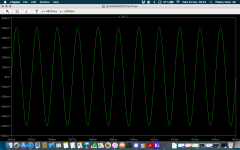
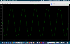
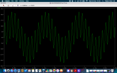
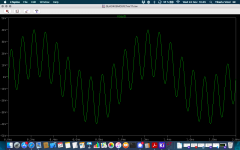
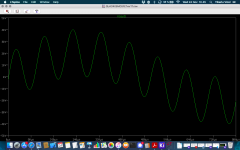
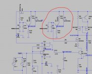
In the process I have also now created a simulation as you demonstrate with 1kHz and 10kHz and looked at the base voltage of Q12. This shows very small pulses which decay ( Fig. 1). According to my analysis these are the feedbacks of the capacities into the Mosfet, so that these play. But since the Q12 is now not there to amplify disturbances of the Mosfet, I have now the following modification (picture 2) to dampen this effect.
Since there are feedbacks from Q8 to the power supply of the OPA, my question is whether a second power supply for Q8 would have disadvantages (picture 3)?
I am still analyzing why one Q17 is playing very excellent, the others not yet at this level.
In the process I have also now created a simulation as you demonstrate with 1kHz and 10kHz and looked at the base voltage of Q12. This shows very small pulses which decay ( Fig. 1). According to my analysis these are the feedbacks of the capacities into the Mosfet, so that these play. But since the Q12 is now not there to amplify disturbances of the Mosfet, I have now the following modification (picture 2) to dampen this effect.
Since there are feedbacks from Q8 to the power supply of the OPA, my question is whether a second power supply for Q8 would have disadvantages (picture 3)?
Attachments
Tim,
If one Q17 is OK, while others not, I would look on what is different between them. Are there same parts ? Are these parts genuine ?
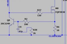
A slow Q8 may improve CCS stability. Move that snubber between transistor collector and base.
Slowing down Q5 also make amplifier much stable. This can be down by adding a capacitor, 100pF or higher, between gate and drain.
Making a separate reference voltage for M9 will not add any benefit.
Regards,
Tibi
If one Q17 is OK, while others not, I would look on what is different between them. Are there same parts ? Are these parts genuine ?
A slow Q8 may improve CCS stability. Move that snubber between transistor collector and base.
Slowing down Q5 also make amplifier much stable. This can be down by adding a capacitor, 100pF or higher, between gate and drain.
Making a separate reference voltage for M9 will not add any benefit.
Regards,
Tibi
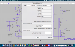
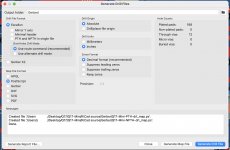
Check your pcb edge cut drawings.
Generate drill file, but there is no need to generate drill map file. Uncheck extended X2 format. Include margin.
HI Tiby!
I got with this new setup.
Q17-Mini-Edge_Cuts.gbr(Board Outline Layer):Gerber file with a board outline
Q17-Mini-F_Paste.gbr(null): Non-gerber274X/excellon formats
Q17-Mini-Margin.gbr(null): Non-critical Gerber file
Q17-Mini-NPTH.drl(null): Non-gerber274X/excellon formats
Q17-Mini-PTH.drl(null):Unrecognized Gerber file
Q17-Mini-job.gbrjob(null): Non-gerber274X/excellon formats
I googled and found that most of theses "warning" are not critical. I also tried "Include NPTH and PTH in the same file". Same error message but for one file.
For X2, seems to do not generate error but in KICAD the wrote "recommended"?
Do we really need the "margin" layer? See the jlcpcb robot answer.
The "holes" seems to be there and called "MULTI(Multi-Layer)".
Sorry for all theses questions but I've not printed PCB since 10 years.
Stef.
.
Attachments
Last edited:

In our case C7 is the capacitor that can change the "note" of amplifier and his outer foil must match with operational output.
The opamp fortress is well protected.
Stef.
.
Attachments
Tim,
If one Q17 is OK, while others not, I would look on what is different between them. Are there same parts ? Are these parts genuine ?
A slow Q8 may improve CCS stability. Move that snubber between transistor collector and base.
Slowing down Q5 also make amplifier much stable. This can be down by adding a capacitor, 100pF or higher, between gate and drain.
Making a separate reference voltage for M9 will not add any benefit.
Regards,
Tibi
Hello Tibi,
It is the same component quality, this was important for me to make sure. Therefore I also built a second layout for the triple variant.
Then the biggest difference is the trace from Q9/Q11 to Q12. This also looks good in your layout. With the very well playing it is like the board uploaded here in the forum the trace far away from the current damping bridge. With the less well playing variants I have drawn this trace directly between the components of the bridge - see post 492.
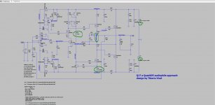
Q17 - a QUAD405 audiophile approach to perfect sound
That Q5 and Q6 can be calmed by capacitors of small size, is out of question. Since I focus on the work of Q12, which should work with particularly low signals, brings me to the idea to damp it. But since I want to influence the signal on the transmission path to Q5 as little as possible, I came up with the idea not to damp Q12 E-C, but Q12 E-B.
My thesis is this: the biggest difficulty with Mosfet is the capacity, I noticed that you always prefer types of Mosfet that have one of the lowest capacities. Now to other effects also arises the issue that with three final transistors the capacity triples. I now ask the question in the room, can this also lead to unwanted distortion and unfavorably affect the feedback on the amplifier? Assuming these feedbacks are those that I attenuate by a snubber at Q12, I should be able to influence the sound quality as little as possible with it....
- Home
- Amplifiers
- Solid State
- Q17 - an audiophile approach to perfect sound