using a supply voltage higher than +-25V would lead to thermal stress for the TDA. So the Amplifier you can get is about 25W@8R / 50W@4R. For home-HiFi this is quite a lot, at least for high efficiency speakers.
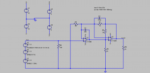
I am about to "tame" the chip with a circuit topology seen in the service manual of SAC (a well known company in german high quality HiFi). The SAC 50 is based on an NE5534 followed by a discrete power stage and a nested feedback... so i tried to adapt this to a composite chip amp, here is the topology, the real world design is in progress....
I am about to "tame" the chip with a circuit topology seen in the service manual of SAC (a well known company in german high quality HiFi). The SAC 50 is based on an NE5534 followed by a discrete power stage and a nested feedback... so i tried to adapt this to a composite chip amp, here is the topology, the real world design is in progress....
Attachments
using a supply voltage higher than +-25V would lead to thermal stress for the TDA.
But then you might as well use the LM3886. It can handle ±30-32 V even with a 4 Ω load.
Tom
If the extra power is needed the LM3886 is for sure an option. But the first thing to test is if the attached circuit topology ist working as simulated in real world design using LM4562 and TDA7293.
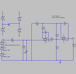
A few more simulation runs showed that the circuit could be further simplified, R2 and R5 are not really needed...
A few more simulation runs showed that the circuit could be further simplified, R2 and R5 are not really needed...
prototype boardwork is done
The prototype boardwork is done. I put the TDA on the edge of the board. But that is only for this prototype, as the pins locations of the TDA is really horrible when mounting it that way.
And as read in several posts in this forum and in neurochromes homepage (taming the LM3886),
there will be room for improvement by shortening the feedbackloop-routes for a more stable operation (thank you Tom) and designing a separate (regulated?) power supply for the input stage of the TDA with a slightly higher (5 to 10V) voltage. This should lower TDAs THD-value (thank you Klaus). As stated above, an edge-mounted TDA is therefore no longer tolerable and work on the direction of the pins needs to be done, because non of the standard pinouts that could be delivered by the distributors are in a direction then needed. But as this is DIY so this is not a problem.
questions and comments to the attached board are welcome.
Bernd
Attachments

With a little work on the compensation network the circuit works. It is 20nF at the error amp (LM4562) and 400pF at the power amp (TDA7296). At 20kHz squarewave there is minimal overshoot at small signal, the -3dB point ist about 400kHz (@3Vpp). The circuit is completely DC-coupled and the resulting output-offset is -6mV. Clipping not yet tested.
But there is also some work to be done, as the amp shows high frequency noise at startup for a couple of ms.
Measurments following as soon as I find the time to do some....
But there is also some work to be done, as the amp shows high frequency noise at startup for a couple of ms.
Measurments following as soon as I find the time to do some....
questions and comments to the attached board are welcome.
hello bernd,
interesting!
do you have a schematic of your test setup?
(or did i miss that?)
stephan
The schematics in detail are not yet posted, just the type of topology that was used. (see a few posts above)
As this not really working (noise at startup) I started simulation again with a complexer feedback, found by reading (again) lots of posts in diy-audio. What I found is a complex feedback that should do significant better in overload, bandwidth and distortion.
schematics of the simulation attached
As this not really working (noise at startup) I started simulation again with a complexer feedback, found by reading (again) lots of posts in diy-audio. What I found is a complex feedback that should do significant better in overload, bandwidth and distortion.
schematics of the simulation attached
Attachments
hi and thanks for the response!
maybe i do not really understand your complex feedback but i suspect that this would not exactly qualify as composite amplifier, as you only use very little negative feedback to drive the correction op-amp.
please do correct me if i'm wrong!
maybe i do not really understand your complex feedback but i suspect that this would not exactly qualify as composite amplifier, as you only use very little negative feedback to drive the correction op-amp.
please do correct me if i'm wrong!
Last edited:
The way I understand composite amplifiers there is one opamp controlling the other in a feedback loop connecting them both as one "black box", and that is the way I did it. And again, with a few more simulations, it seems that the resistors R4 and R9 are not really needed and R3 can be a piece of wire. So the only differences to the circuit posted before is R5 that is added and the value of C1 is mow really small. The C parallel to R1 (at least in simulation) is no longer needed for a stable amp.
A similar topology is described in an application note about composite amps by Linear Technology (AN21) in 1986.
So I am going to change my circuit as described and will see if it does any better...
A similar topology is described in an application note about composite amps by Linear Technology (AN21) in 1986.
So I am going to change my circuit as described and will see if it does any better...
Last edited:

time to ask the right questions
As we want to get most out of the TDA7293 (and cousins TDA7294/5/6) and we assume a composite amp is the best way to do this (as Tom showed it is possible with his modulus series) it is time to ask the right questions.
The thermal resistance of the TDAs case is relatively high, so for driving a 4 Ohm load it is wise to choose the supply-voltage not too high. An output voltage 50Vpp will be a nice number to start with.
Now take a look at the output swing possibilities of the input/error-amp. They are seldom rail to rail and usually powered by +/-15V. A maximum output voltage of 25Vpp of this amp seems realistic.
And as the following power-opamp has a relatively low GBW-product it should be configured at the lowest possible gain. Now TDA7293s datasheet says on page 6 this number is 20 (26dB). Assuming that this number is for the non-inverting circuit shown in the datasheet, the number for the inverting case will be 10 (20dB).
Looking at the numbers 50Vpp and 25Vpp and wanting a high bandwidth for the power-opamp, choosing factor 2 (6dB) will be the right number. Could this really work? Asking the simulation on an IC that is internally compensated for a gain of 25 says this could work. FauxFrench showed how this is possible for inverting gains of 3 and 5 with several real world power opamps. And simulation shows how to get there: design an non-inverting circuit with feedback resistors of equal value (1k Ohm for example), then add another resistor with a relatively low value between the negative and the positive input of the opamp. Adjust the resistors value to get the broadest bandwidth with no peaking at high frequencies. And when i understand the several application notes the right way, the bandwidth that shows up then will also be the maximum bandwidth for the error amp with his adjusted gain.
So the described way is the next step for me and my project
[sorry for my english - i am not a native speaker]
questions and comments to the attached board are welcome.
Hmmm... To comment or not to comment. That is the question. Well. You did ask... 🙂
The layout looks like a connect-the-dots layout. It'll probably work OK, but there's plenty of room for optimization. If you're going for low THD, I recommend optimizing the layout. The layout is the circuit.
What's the deal with the vias peppered all across the board? Are you using internal layers as well as the two layers shown?
My suggestions:
- I suggest looking at where the large currents flow and optimizing the layout around that.
- I would get rid of the star ground and use a ground plane. Just make sure to keep the quiet grounds in a quiet area of the plane. You can do this by moating (careful!) or by having multiple ground layers (and ensuring that you don't accidentally connect a "loud" ground on the "quiet" layer.
- Same applies for the power supply rails. You pay for the copper anyway. You might as well use it!
- There's really no reason to use SMD bypass caps. If you do go that route, I suggest using 0805 or 1206 sized caps as the tiny ones tend to have pretty steep voltage coefficients (the larger ones do too, it's just not as horrid). You'll definitely want an X5R or X7R dielectric cap there.
- I suggest using a regular mounting hole pattern. Currently you have the holes wherever they'd fit. You'll hate yourself for that when it becomes time to drill holes in the chassis. I'd also put a couple of holes by the edge of the board that goes against the heat sink. If you plan to use a ModuShop chassis, you might consider making the hole pattern in your board fit their 'holey' internal plate.
- The reservoir capacitors look tiny. You'll probably want 10000-22000 uF there.
- You only need one rectifier. Also, there's no practical reason the snubber cap can't be a leaded part. That would allow you to use a film cap, which would be better for snubbing.
The last two points might warrant spinning off the power supply as a separate board. There are advantages to having the power supply on the amp board - but there are also disadvantages.
I do like that you laid the two TO-220 packages flat against the board. Bonus points for that! I'm not a fan of standing those up unsupported. That's a recipe for failure. Much better to put them against the board and secure them with a screw as you've done.
I also like that you brought the power supply in from one side rather than both as you often see in (suboptimal) LM3886 layouts.
I'm not intimately familiar with the TDA7293, so take this bit of advice accordingly: I would look at the current draw of the input stage and see if the 100 mA version of the LM317/LM337 (LM317L and LM337L, respectively) can be used.
Be careful with the supply voltage. The LM317/337 are limited to 37 V differential (Vin-Vout).
I put the TDA on the edge of the board. But that is only for this prototype
I would design the board as if it's the final version. My first Modulus-86 prototype layout looked very much like your layout. I put it together pretty quickly as a proof of concept. It provided hardly any useful data as the layout dominated the performance. It did spur a range of experiments related to grounding, though, so it wasn't all for naught.
Tom
Last edited:
Thanks for your comment Tom.
You are right - the layout is the circuit. And grounding the right way seems not so easy - I have seen this at this prototype by testing the idea of +6dB for the TDA. At a first look to sinewave it seems to work fine. Switching to squarewave showed the problem of the layout - on 0V and on DC level of the squarewave I could see a little ringing (approx. 1mVpp/2MHz). Changing the grounpin from the feedback-network directly to the speaker ground eliminated the ringing on the DC-Level, but the ringing on the 0V did not dissapear. By changing the input ground to the speaker ground too, the ringing at 0V level also dissapeared. A precise look to the layout showed the cause: the signal ground shared the power ground of the TDAs input-stage power supply bypass-caps.
The +6dB works as expected. Typing "composite amplifier stability" into the internet search engine showed a lot of hints, and in the datasheet of AD8067 on page 21 it is shown how to calculate the value of the resistor between the inputs...
Attached some screenshots of the TDAs +6dB circuit. As they are named, I think there is no further comment neccesary. Otherwise do ask....
Attachments
-
 X-Y-200kHz.png36.6 KB · Views: 122
 -
 X-Y-20kHz.png36.1 KB · Views: 129
 -
 X-Y-2kHz.png34.3 KB · Views: 110
 -
 X-Y-200Hz.png34.3 KB · Views: 334
 -
 200kHz-phaseshift-sinewave.png42.8 KB · Views: 335
 -
 squarewave-response-fall-gen-amp.png38.1 KB · Views: 329
 -
 squarewave-response-rise-gen-amp.png36.8 KB · Views: 328
 -
 non-inverting-6dB-gain.png39.4 KB · Views: 375
Further comment definitely is necessary as the graphs aren't labeled. It would be nice to have input and output marked on the step response and some explanation of the XY plots.
Tom
Tom
Hello Tom,
first some answers to your questions
- the vias peppered across the board are connections from bottom to top of the two layer board - its a copper pour connected to ground intended as a shielding. The copper pour is not shown for clarity.
- the smd parts used are X7R and surely i have to take a look into the datasheet if the bigger parts do better
- the reservoir capacitors are 4700µF by the rule of thumb to have at least 1µF per 1mA of the current expected, some more sure do better
- the intention to use 2 rectifiers came from the idea to break the groundloop when using 2 ore more boards with the same transformer and RCA phono plug inputs.
This could also be done by adding two antiparallel diodes between the power supply ground and each board ground. But if it really works this way is not yet tested.
- reason for using LM317/LM337 in TO220 is the price, which is half the price of the ones in TO92, at least at my favoite distributor. In the end i have to calculate if the cost for the little extra board space needed would justify this decision
- I am aware of the maximum input voltage for the LMs and have in mind to put some Z-diodes in series to their input if i go higher in voltage than allowed for them.
If the prototype is the final version it will be fine - and it often works that way just looking at the function itself, but getting most out of the circuit - and that is the
intention here - a little more work has to be done.
Now the comments to the graphs (with detailed description, especially for the noobs):
graph1:
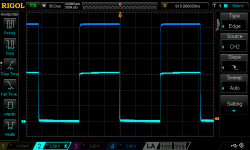
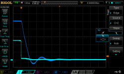
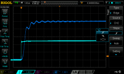
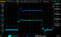
the cyan coulored line shows the output of the waveform generator and the blue one is the output of the amp. The oscilloscopes inputs are switched to the same value per division to show that the amplification is non inverting +6dB. The squarewave was chosen to see if there is any overshoot which (if present) is a sign for instability. the amplifiers load was 8 Ohm, Zobel-circuit at the amps output, no Thiele circuit. 0V at the bottom of the squarewave, so only the "upper half" of the amp is tested.
graph2:
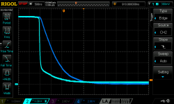
coulors, squarewave and load are the same as in graph one, but the sensitivity for the generators output (cyan) is doubled and the timebase is changed to see the amplifiers reaction to the fast rising edge.
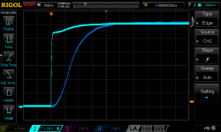
You can see high frequency limiting of the amplifier (rising edge of the amplifier is slower than the generators rising edge). Taking a closer look to the lower corner you can also see the time it takes for the amplifier to react (group-delay), in this case roughly 100ns.
graph3:
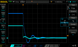
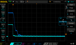
same as graph2 but for the falling edge of the squarewave
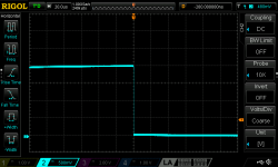
graph4:
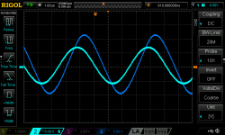
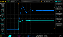
coulors as before, showing the generators and amplifiers output at the frequency of 200kHz. You can see the reduction of the amplifiers output and that there is some phaseshift (timedelay) between in and out.
hardly visible here: the shape of the sinewave on the amplifiers output changed. [not shown here: the amplifiers output at 200kHz at higher output levels gets closer to the shape of the triangle the higher the level - that is what Douglas Self calls "slewing induced distortion" and could be expected as the slewrate for the TDA is only 10V/µs. The datasheet of the LM3886 shows the same number and i expect it does no better at this test]
graphs5,6,7,8:
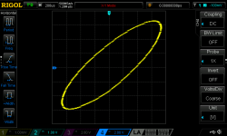
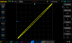
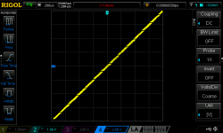
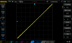
oscilloscopes inputs as above, but function switched to XY-Display. sinewave-testing for the frequencys 200Hz (graph5), 2kHz (graph6), 20kHz (graph7) and 200kHz (graph8). The sensitivity for the generators output is doubled to get the line into the angle of 45° (if the scopes inputs are switched to the same sensitivity, the angle would be 22,5° in respect to the vertical because of the 6dB amplification). what can be read out of this kind of display is the phaseshift of the signal: you will see a line at 0° and as the phaseshift rises the shape of the line changes and shows a circle at 90° phaseshift.
shifting the phaseshift further to 180° you will again see a line, but in the opposite quadrants of the display.
in graph7 for example, you can see that there is a little phaseshift at 20kHz which you wouldn't probably notice by just looking at the sinewaves.
in graph8 you can see, that phaseshift rises as frequency rises. it is taken at a low output level. When rising the level here, you can also see the oval changes his shape for the amps output sinewave changes to triangle.
Bernd
first some answers to your questions
- the vias peppered across the board are connections from bottom to top of the two layer board - its a copper pour connected to ground intended as a shielding. The copper pour is not shown for clarity.
- the smd parts used are X7R and surely i have to take a look into the datasheet if the bigger parts do better
- the reservoir capacitors are 4700µF by the rule of thumb to have at least 1µF per 1mA of the current expected, some more sure do better
- the intention to use 2 rectifiers came from the idea to break the groundloop when using 2 ore more boards with the same transformer and RCA phono plug inputs.
This could also be done by adding two antiparallel diodes between the power supply ground and each board ground. But if it really works this way is not yet tested.
- reason for using LM317/LM337 in TO220 is the price, which is half the price of the ones in TO92, at least at my favoite distributor. In the end i have to calculate if the cost for the little extra board space needed would justify this decision
- I am aware of the maximum input voltage for the LMs and have in mind to put some Z-diodes in series to their input if i go higher in voltage than allowed for them.
If the prototype is the final version it will be fine - and it often works that way just looking at the function itself, but getting most out of the circuit - and that is the
intention here - a little more work has to be done.
Now the comments to the graphs (with detailed description, especially for the noobs):
graph1:
the cyan coulored line shows the output of the waveform generator and the blue one is the output of the amp. The oscilloscopes inputs are switched to the same value per division to show that the amplification is non inverting +6dB. The squarewave was chosen to see if there is any overshoot which (if present) is a sign for instability. the amplifiers load was 8 Ohm, Zobel-circuit at the amps output, no Thiele circuit. 0V at the bottom of the squarewave, so only the "upper half" of the amp is tested.
graph2:
coulors, squarewave and load are the same as in graph one, but the sensitivity for the generators output (cyan) is doubled and the timebase is changed to see the amplifiers reaction to the fast rising edge.
You can see high frequency limiting of the amplifier (rising edge of the amplifier is slower than the generators rising edge). Taking a closer look to the lower corner you can also see the time it takes for the amplifier to react (group-delay), in this case roughly 100ns.
graph3:
same as graph2 but for the falling edge of the squarewave
graph4:
coulors as before, showing the generators and amplifiers output at the frequency of 200kHz. You can see the reduction of the amplifiers output and that there is some phaseshift (timedelay) between in and out.
hardly visible here: the shape of the sinewave on the amplifiers output changed. [not shown here: the amplifiers output at 200kHz at higher output levels gets closer to the shape of the triangle the higher the level - that is what Douglas Self calls "slewing induced distortion" and could be expected as the slewrate for the TDA is only 10V/µs. The datasheet of the LM3886 shows the same number and i expect it does no better at this test]
graphs5,6,7,8:
oscilloscopes inputs as above, but function switched to XY-Display. sinewave-testing for the frequencys 200Hz (graph5), 2kHz (graph6), 20kHz (graph7) and 200kHz (graph8). The sensitivity for the generators output is doubled to get the line into the angle of 45° (if the scopes inputs are switched to the same sensitivity, the angle would be 22,5° in respect to the vertical because of the 6dB amplification). what can be read out of this kind of display is the phaseshift of the signal: you will see a line at 0° and as the phaseshift rises the shape of the line changes and shows a circle at 90° phaseshift.
shifting the phaseshift further to 180° you will again see a line, but in the opposite quadrants of the display.
in graph7 for example, you can see that there is a little phaseshift at 20kHz which you wouldn't probably notice by just looking at the sinewaves.
in graph8 you can see, that phaseshift rises as frequency rises. it is taken at a low output level. When rising the level here, you can also see the oval changes his shape for the amps output sinewave changes to triangle.
Bernd
I have to add a thing, the board i actually work with is the previous version of the one that is shown - therefore, the described ringing at 0V and DC-Level at squarewave-testing would not show up with the board that is shown...
(...it was not meant to be that way, but i really did order the wrong version of the board...)
(...it was not meant to be that way, but i really did order the wrong version of the board...)
I would terminate the signal generator in 50 Ω (assuming it has 50 Ω output) for the square wave test. Your square wave is pretty distorted. The output of the amp looks well controlled. I suggest adding a capacitor in parallel with the resistive load. I usually go three steps per decade (1.0, 2.2, 4.7) starting at 1 nF and ending at 4.7 uF. I like to see a well-behaved amp with 1+ uF load.
Interesting with the XY graphs, but note that they don't say much (if anything) about stability.
Tom
Interesting with the XY graphs, but note that they don't say much (if anything) about stability.
Tom
Yes, terminating the input with a resistor value of the cables impedance will show a better squarewave, even if the generators output impedance is not matching. Correctly terminated no energy will be reflected. I will do the measurements again with a signal cable with a defined impedance and termination and willalso add caps parallel to the output as you suggest.
By the way: I was wrong with the LMs slewrate as i had his minimum specs in mind. As its typical slewrate is almost twice the TDAs value it will be the better choice at the end.
Bernd
By the way: I was wrong with the LMs slewrate as i had his minimum specs in mind. As its typical slewrate is almost twice the TDAs value it will be the better choice at the end.
Bernd
some more data
for all graphs: cyan is the amps input , blue is the amps output
graph1:
75 Ohm Generator out connected to a 50 Ohm cable terminated with 50 Ohm at the amp-input, measured at the amp input by a 10:1 probe
graph2:
graph3:
load to the amp 8 Ohm || 10nF
graph4:
graph5:
load to the amp 8 Ohm || 100nF
graph6:
graph7:
load to the amp 8 Ohm || 1,5µF
graph8:
load to the amp 8 Ohm || 10µF
looks good to me, except the 8 Ohm||10nF measurement that shows some ringing...
Another thing i did not expect is the distortion of amps input when adding caps to the output...
Attachments
-
 TDA-6dB-step-fall-8R-1u5.png36.4 KB · Views: 90
 -
 TDA-6dB-step-rise-8R-1u5.png35.4 KB · Views: 92
 -
 TDA-6dB-step-fall-8R-100n.png36.2 KB · Views: 104
 -
 TDA-6dB-step-rise-8R-100n.png36.3 KB · Views: 98
 -
 TDA-6dB-step-fall-8R-10n.png35.9 KB · Views: 115
 -
 TDA-6dB-step-rise-8R-10n.png36.2 KB · Views: 99
 -
 gen-out-75-amp-in-50.png33.4 KB · Views: 109
 -
 TDA-6dB-step-8R-10u.png36.7 KB · Views: 104
another question that came into my mind:
what is the ideal cable to connect the amplifier to the loudspeaker from the technical sight? (assuming 10ft / 3m length)
I actually use 2x0,75mm² standard speaker cable that i twisted.
I experimented with a shielded 2x0,75mm² and saw on the oscilloscopes screen, that the shielding works more like an antenna than like a shield (shield connected to the circuits ground)...so this is not the way.
therefore:
what is the best way to bring the high quality of an amp to the speakers voice-coil?
Is shielding necessary / useful? If yes, how should it be done? If no, why not?
- Home
- Amplifiers
- Chip Amps
- TDA 7293 -- done right ?