Thank you Prasi,
as I simulated with 1K R3 both options work fine. slightly different gain. I don't know how NP finally selected resistors - if the NP PCB does not contain R35. probably everyone has their own choice
as I simulated with 1K R3 both options work fine. slightly different gain. I don't know how NP finally selected resistors - if the NP PCB does not contain R35. probably everyone has their own choice
I've read the majority of the thread so apologies if I missed it. I have taken delivery of Prasis AB100 layout.
If I am reading the schematic and board right then R16 10.1 is linked to F1 via jumper wire J3. Thick white line along the top edge.
Looking at my board J3 doesn't go to F1 but to GND.
Do I need to do a little modification?
The stuffing guide image i have been referring to is the same as my PCB.
I'm sure this is my inexperience and not an error!
Attachments

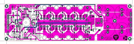
That is a ground trace coming from the input side, since your pcb are already manufactured double sided, there is no need for any jumpers or modification, there is already a trace on top copper. Board is fine as is.
For singled sided diy etching of pcb, jumpers are required.
refer this post regarding value of R3.
AB100 Class AB Power Amplifier
For singled sided diy etching of pcb, jumpers are required.
refer this post regarding value of R3.
AB100 Class AB Power Amplifier
Wish you good luck! better to ask a question than to burn transistors.
Very good sounding amplifier and cool - considering that in my city +30 C
Very good sounding amplifier and cool - considering that in my city +30 C
Thanks for the feedback. I'm planning on using a 35v trafo which will give me just under 50vdc on my mains.
I chose AB100 and also FH9 as the rail voltage matches my current 3255 class d @50vdc. So I can swap my power amps with the same trafo. Admittedly different psu for dual rail on the AB amps..
Thanks for all the help so far. Big mouser order placed.
Thanks for all the help so far. Big mouser order placed.
I chose AB100 and also FH9 as the rail voltage matches my current 3255 class d @50vdc. So I can swap my power amps with the same trafo. Admittedly different psu for dual rail on the AB amps..
Thanks for all the help so far. Big mouser order placed.
Would you care to share your Mouser cart?
I am curious to see what components you chose.
I can share my last order. However it isnt itemised as a BOM and there are a couple or three projects in there. It will take me a while for me to fathom what I ordered goes where, nevermind yourself!
you may use MFR from your bin. No need for separate mouser order.
For critical components like FB cap, input cap, etc, use good quality
For decoupling bulk cap, use from your bin.
For critical components like FB cap, input cap, etc, use good quality
For decoupling bulk cap, use from your bin.
Thank you Mr. Pass , Prasi , Oscar and everybody else who has contributed to this thread . 🙂
I have a couple of questions regarding part choices :
1. Is it OK to substitute KSA1381/KSC3503 for 2SA1380/2SC3502 which are available in South Africa ? Dissipation 7W vs 5W ; Max VCBO ±200V vs ±300V
I see the devices Mr Pass initially specify - 2SA1110/2SC2590 have even lower Max VCBO ±120V .
2. I have 2 types of BD139 , BD139_10 (Hfe 60-160) and BD139_16 (Hfe 100-250) . Would BD139_16 be the better choice ? That seems to be in the ballpark of the original ZTX450 .
3. I got ON TIP142G & TIP147G (TO-247) , I see Jan got MJ's , I'm wondering if I should sell the TIP's ? Edit : Oops ! I see Jan replaced the MJ's with 2SA/2SC
4. I got the recommended BC547/557 B-rated , any better recommendations ?
Thanks guys !
Last edited:
Hallo Ari, NO do not sell the TIPs, I have used them , maybe a mis understanding or mis wrote.😉
RS Components | Electronic and Electrical Components
I have used BD139-16
RS Components | Electronic and Electrical Components
I have used BD139-16
Last edited:
Thanks man Jan ! I realize now I can't actually afford to get other output devices at this point anyway .
I have both BC547/557 and BC550/560 , the latter seem to be the 'low noise' component .
I have both BC547/557 and BC550/560 , the latter seem to be the 'low noise' component .
Ari, you can use either of them , use the one with the highest gain. (Hfe) I think I used the BC547.
I need to build a summer amp, so here is my plan with parts I have on hand
Each heat sink is 6"H x 7 1/4" long or 152.4 mm x 184.15.
The only thing that makes me nervous is the seam in the sinks and if that is going to create a hot spot and be problematic.
Each heat sink is 6"H x 7 1/4" long or 152.4 mm x 184.15.
The only thing that makes me nervous is the seam in the sinks and if that is going to create a hot spot and be problematic.
1% MFR tolerance itself is +/-0.22kOhm for 22kOhm nominal value, so there is no problem using 22k
- Home
- Amplifiers
- Pass Labs
- AB100 Class AB Power Amplifier