fuses blow
While testing, I suggest to replace R153 by much higher value resistors, e.g. a pair of 1K/5W. That way the output current can never exceed 40mA and your last two fuses should hold.
If you can do that for both channels, you can compare voltages, e.g. drop accross R146 for L and r channel>
Then try shorting c/e Q107, which effectively shorts the powerstage drive. If there was excessive current drawn (excessive being 40mA through the output transistors), that current should drop to virtually 0.
If it drops to 0, output stage is likely OK.
Then check Q107 as it may be "open". When in doubt, replace it by any NPN with Ic > 100mA
Roger, buy transistors from authorized distributors like newark digikey mouser arrow alliedelec (in USA).I pulled the output transistors and they passed every test I could think of. I just don't see any shorts and I tool Vceo up to 17V. But if I do need to replace them, are these (B863 and D1148) things unobtainium? It sounds like the ones for sale on eBay are fakes.
Probably the old output transistors are fine. But I'm not going to look them up, ancient history. Emitter followers, as long as the package matches, the Vceo is equal or higher, the Ic is equal or higher, and no weird features like the .15 emitter resistor built into a homotaxial 2n3055 (1964-1976) then nearly anything will do. My stock replacement TO3 is MJ21193/21194 which are cheaper than MJ15024/25. For this you could probably save $1 each and use MJ15015/16. Latter probably not in stock. Details of the temperature pickup transistor resistor network may have to change to make the idle current right.
Update the mica washer, & compound, mica has a service life of about 40 years or x0000 temperature cycles. Silicon rubber requires no thermal grease but newark never has any in the precut sizes I need. The others cost more freight to my location and have non-ideal electrolytic capacitor practices so I use newark mostly.
Last edited:
Interesting test idea Athelas. I have some 1k/5W resistors in the parts cabinet and should be able to kludge up a high resistance version of R153.
I will also take another look at Q107. I know it is not C-E shorted, but I did not check to see if it is blown and failed open. If Q107 failed open it looks like Q105/Q106 would drive the positive output transistors Q108/Q110 ON, and likewise R150/R151 would pull down the base Q109 and force Q111 ON.
Q110 and Q111 both ON at the same time would definately blow F1 and F2.
Thanks for all your help folks. After decades of FPGAs and VHDL the rusty creaky old school analog wheels are beginning to turn again...
The bases of Q108 and Q109 need to be held apart by approximately 2.4 v. The result of the success of this is a current through Q110 Q111 at idle (input shorted) of 20 ma to 40 ma. (If they are TO3). If the voltages are further apart, too much cross current will flow. That would cause the output transistor to overheat.
I'm not suggesting any particular modification to the q107 network, but that network must produce these idle bias currents to both avoid crossover distortion (switching noise) and overheating. One checks the current through Q110 111 by the voltage across R153.
This is a normal check at the end of the repair process. The voltage check between the two bases Q108 Q109 should be an early check of the circuit.
Those Kicad schematics sure are a lot prettier -- thanks for taking the time and effort to do those.
Um .. err .. are the pinouts of Q301, 303, and 305 correct? Haven't seen too many transistors from Japan that have the Emitter on pin 2.
Q107 doesn't need removing to check for Failed-Open -- as long as R150 and R151 are yanking down hard, either there's enough leakage from the VAS, or you can touch just about any 2k2 - 10k resistor from Q107-C to ground. Then measure from there to the other driver Base (across the driver Bases) looking for that magic 2,4V value.
Incidentally, the difference in resulting symptom between Q107 Failed-Open and Failed-Short is the reason wise designers put the trimpot across the Base-Emitter span of the resistive divider. 😉
Regards
Last edited:
The pin numbers are not correct in the schematics... I need to find a way to turn those off in KiCad. Thankfully the 3125 PCB is fairly well designed and each transistor has the leads clearly marked on the silkscreen. Which is good because it seems like TO92 and TO220 pin numbering is totally arbitrary.
In a previous post it was recommended to leave Q110 and Q111 out and in their place tack a diode on the B-E pads. I have not tried that yet, but wouldn't that be the same thing as putting Q110 and Q111 back in but leave C disconnected? I have previously tested Q110 and Q111 out of circuit and the B-E junction looks OK.
In a previous post it was recommended to leave Q110 and Q111 out and in their place tack a diode on the B-E pads. I have not tried that yet, but wouldn't that be the same thing as putting Q110 and Q111 back in but leave C disconnected? I have previously tested Q110 and Q111 out of circuit and the B-E junction looks OK.
Are these TO3 output transistors? Leaving C disconnected means not placing the transistor on the heat sink, and that endangers them if the cross current is 1 or 2 amps. Even for a few seconds. I'd just put them back, let the 40 w bulb limit the damage, and measure idle bias current or Q107 voltage quickly. I use an outlet strip in front of me to give me quick access to the AC power switch.
If you don't have any diodes, and don't want to spend $9 freight to get some for $.07 each, take apart some old appliance like a radio phone or something. They are full of them. Even box fans or ovens can have them. dead PCAT switcher supplies are full of those and other useful things, too.
If you don't have any diodes, and don't want to spend $9 freight to get some for $.07 each, take apart some old appliance like a radio phone or something. They are full of them. Even box fans or ovens can have them. dead PCAT switcher supplies are full of those and other useful things, too.
Last edited:
Q110 Q111 and Q107 are mechanically connected to the heat sink but are all electrically isolated. The bracket for Q107 is pretty kludgy and if one is not careful the TO92 could get pushed deeper into the bracket and risk shorting out the leads (heatsink is chassis ground). I did not see any evidence of this happening though.
Attachments

Those leads are cut long enough you could take two alligator clip leads to bases of the two output transistors. I think the bases are on the right from the bottom. Meter on 20 v scale, turn the AC on and turn off again as fast as reading stabilizes. > 2.7 v between bases, Q109 or resistor network has a serious problem. Reading about 2.4 v, then measure across R153 next time AC on. Across both resistors 8 mv to 2 mv, across only one half 4 mv to 1 mv.
Fusible Resistors
A number of resistors have the prefix FR which disappeared in the tidy up versions of the schematic. If FR152 has failed the voltage between the bases of the output transistors would be higher causing a substantial increase in output current. All FR designated resistors should be checked to see if any has fused.
A number of resistors have the prefix FR which disappeared in the tidy up versions of the schematic. If FR152 has failed the voltage between the bases of the output transistors would be higher causing a substantial increase in output current. All FR designated resistors should be checked to see if any has fused.
Attachments
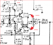
Checked the fusable resistors and they are OK. Output transistors Q110 and Q111 are back in (C is not connected). I'm getting the 2.4V across bases Q108 and Q109 as shown. Q108 and Q109 starting to get toasty and beginning to pull down the +/-28V rail. Hmm...
Attachments
Umm .. Except, if an Emitter resistor has failed Open, there's no path for the current to increase. It's a handy way to roughly estimate the health of the bias circuit, without putting the output devices at risk .. Or buying a pile of fuses .. Or wearing out the Variac or the dim bulb tester .. 😉
Cheers
edit: this was responding to post 32; will take me a few minutes to sort #33
Cheers
edit: this was responding to post 32; will take me a few minutes to sort #33
Last edited:
What is the voltage across the two legs of R153 to BK101?
If +28 is collapsing, perhaps Q108 is leaking. Voltage above should show it. Could be Q106 bad, voltage across 68 ohm resistor fr146 should show if that current is excessive.
If +28 is collapsing, perhaps Q108 is leaking. Voltage above should show it. Could be Q106 bad, voltage across 68 ohm resistor fr146 should show if that current is excessive.
We're getting closer to the real problem, then! 😉 There shouldn't be enough current demand to more than slightly warm the drivers, let alone yank down the high-current 28/34 volt supplies.
Is the 4/8 ohm switch in the 8 ohm position, by any chance? What is the dim bulb tester saying at this point?
What voltage do you show across FR152? What voltage from it to ground? (In other words, is the feedback loop doing its job?)
Cheers
edit: Oops -- indianajo beat me to it .. 😱
Is the 4/8 ohm switch in the 8 ohm position, by any chance? What is the dim bulb tester saying at this point?
What voltage do you show across FR152? What voltage from it to ground? (In other words, is the feedback loop doing its job?)
Cheers
edit: Oops -- indianajo beat me to it .. 😱
Yes getting closer...
Speaker in 4 ohm position. High current rails are +/-26.5V
Q109 B = -1.3V, E = -0.7V
Q108 B = 1.15V, E = 0.5V
So across FR152 I've got 1.2V, or about 5mA flowing through that resistor.
Quick check shows three legs of R153 are sitting at -0.1V
Hold on... I may be looking at a bad solder joint somewhere. Pressing on the board makes the 40W dim bulb glow and dim. Will touch up all the solder joints and in L and R channel amp sections now.
More profitable is taking more voltages to speaker ground from the component leads. Usefully, touching component leads with the meter probe often makes the dim bulb go out. If so, bingo! that lead is the problem. Write down the voltages you take, as you've done here prviously. The problem may not be obviousl, but after you stare at the print with voltages improbable readings lead to analysis.Hold on... I may be looking at a bad solder joint somewhere. Pressing on the board makes the 40W dim bulb glow and dim. Will touch up all the solder joints and in L and R channel amp sections now.
If voltage on the component leads at two ends of circuit trace are different, you've found the bad solder joint. No point in touching up the others, they were made by pros. Meanwhile, the voltages themselves tell you something about the components. Vb>Ve of a transistor more than ~.7 v, it is likely open. voltages at two ends of a resistor > that allowed by wattage rating, it is blown. (experience will tell you what wattage rating is by size). V^2/R=P.
Voltages across both leads of a capacitor the same, it is likely shorted. etc.
Happy hunting.
Last edited:
Checked the fusable resistors and they are OK.
Did you check FR1 and FR2 in the power supply?
Well after going through both amp sections with a soldering iron and touching up all the solder joints the voltages around Q108 and Q109 started to look more consistent across L and R channels. So I fully connected the output power transistors Q110 and Q111. And both channels seem to be working now. No hot smell, no magic smoke. Everything seems to be running cool. Adjusted VR101 for 0V at the output OK. Adjusted VR102 for 2mV across R153 OK. Switched out the dim bulb and hooked back up the regular AC mains. Let it sit to discharge the caps, then turn it on. Cycle power a bunch of times. All fuses seem to be holding. 🙂
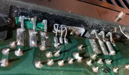
Huh. Maybe it was just a crap solder joint after all. This NAD amp was manufactured in Japan in 1985. The overall quality of the solder joints is OK but there was a shocking amount of solder flux left on the board. Doesn't look like it was cleaned at all after going through the wave soldering machine. Maybe that was OK in 1985 but it wouldn't fly today.
Anyway, close it up tomorrow and put it through it's paces with better speakers attached. I'll update the schematics and post them here to help others who have been asking for the NAD 3125 details. Thanks for helping a digital guy re-discover the elegance of old school analog.
Attachments
- Home
- Amplifiers
- Solid State
- NAD 3125 blown fuses and output transistors