OK, looks like it is good to have checked the emitter resistors.
One channel, all emitter resistors all about 165mV so I assume it's OK
Other channel: emitter resistors on NPN all about 200 mv BUT the PNP emitter resistors not the same: 4 (R9 R13, R17, and R21) are about 100 mV But R25 is only about 5 mV
Seems like a problem, but I'm not sure what to check. I will pull the board and check component orientation and solder joint
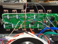
Looks like I might have found the problem. There's a defect in the board and the pads of R25 are shorted together. Apparently the board wasn't trimmed properly and there's a piece of trace running along the edge of the board that shouldn't be there.
I bought 5 boards and four are fine. Naturally I picked up the problem board...
I bought 5 boards and four are fine. Naturally I picked up the problem board...
Good you found that problem and would explain your measurements.
Have just checked my O/S boards around that resistor and all are fine.
Once fixed, it will be interesting to see what you measure now across the emitter resistors and how that relates to both heatsink temps.
Can you tell me what your ambient temp is with 50 deg C on the heatsinks, and what the final bias current is on each channel.
With previous measurement of 190mA per device at 35 volt rails is only 6.7 watts dissipation per output transistor - around a total of 80 watts dissipation for each channel's heatsink. That is well and truly inside the SOA DC curve for the Sanken's.
Yes, it appears to have corrected the problem. All emitter resistors measuring about the same voltage drop (within 5 or so mV.)
I don't know that I will get it fully adjusted tonight as it's late here.
Before I fixed this, here's what I had on working channel: about 190mV; heatsink temp about 47C and ambient temp 19C.
I'll report final answers as soon as I get them.
I don't know that I will get it fully adjusted tonight as it's late here.
Before I fixed this, here's what I had on working channel: about 190mV; heatsink temp about 47C and ambient temp 19C.
I'll report final answers as soon as I get them.
Where did you get your boards made - I will have to check mine.
JCLPCB.
Attached is a parts list and my build notes. I used a PSU board designed by Jeff Young. 22,000mfd per rail. 2, 300VA-25 V transformers from Antek.Has anyone completed one of these amps yet and have a parts list used for the power supply and driver boards (transistor models)?
Attachments
Attached is a parts list and my build notes. I used a PSU board designed by Jeff Young. 22,000mfd per rail. 2, 300VA-25 V transformers from Antek.
Thanks, so you did not use the OS boards that ZenMod posted? I was also wondering about which output transistors work on those boards.
Yes he used the 6 pair ZM O/S boards as shown in his photo.
Mine were the same supplier.
Take your time with the final biasing - looking forward to your figures.
30 deg C rise above ambient is good.
Mine were the same supplier.
Take your time with the final biasing - looking forward to your figures.
30 deg C rise above ambient is good.
Looks like I might have found the problem. There's a defect in the board and the pads of R25 are shorted together. Apparently the board wasn't trimmed properly and there's a piece of trace running along the edge of the board that shouldn't be there.
I bought 5 boards and four are fine. Naturally I picked up the problem board...
good to know that my files are OK
🙂

Not quite finished adjusting bias. I had one of those days that you're not supposed to have when you're retired...
But it's close. Up to about 47C with bias on both sides about 220mA. And no smoke!
But it's close. Up to about 47C with bias on both sides about 220mA. And no smoke!
Less heatsink temp and more bias current than previously - how did you manage that?
Good to hear the "no smoke" part.
Good to hear the "no smoke" part.

I have no idea. The only difference is that now all emitter resistors are showing the same drop - previously the NPNs were showing twice the drop as the PNP (except for the one with shorted emitter resistor). I'm now testing with top cover on case and maybe that makes a difference.Less heatsink temp and more bias current than previously - how did you manage that?
Good to hear the "no smoke" part.
when I'm short (often) with explanations, I blame Gremlins
what's important is that you understand present situation, and - of course, that you found what was culprit of previous problems
good work..... waiting for your impressions - does it sing 🙂
edit: regarding pic from #743
output transistor screws - bigger washers and (I hope you have these at least) spring washers, are nice to have, for better sleep
thermal cycling is tricky thing ......
Last edited:
- Home
- Amplifiers
- Pass Labs
- New Stasis front end