Hello to all,
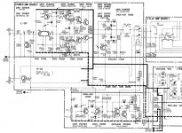
I have run into problems restoring a Sony TA-3650 integrated amp. I replaced the blown right channel output transistors and the driver and bias stage (Q352-Q358) plus the differential pair (Q351). When I turned the amp on after the repair, the rail resistors R356, R370 (fusible 0,25W resistors as it seems to me), burnt (see attached part of the schematics).
I checked the outputs Q57, Q358 again and found one open and one shorted on all junctions each (can’t remember which at the moment). I replaced the rail resistors (with none fusible metal films 0,25W) and powered on without the output transistors, both resistors burn.
I checked Q302-304 and Diodes D301-D303 which seemed to check ok. I nonetheless replaced D302 (infamous “death diode” VD1221). could not spot other resistors which seem burned. The bias pot is set at 7K (as on the good left channel).
I went back and forth through this testing yesterday and smoked the rail resistors a couple of times after checking and test-wise substituting a couple of parts (I swapped the bias diode D303 against 4 normal diodes in series as suggested somewhere else here but to no avail. I even swapped C352 and C357 against new ones. The whole amp is in for a recap if I can find and repair the fault).
Now I am clueless. Where is my mistake?
I don’t get where the rails are shorted together (as it seems they must be, and must be after, not before the rail resistors; so obviously no short through the driver transistors).
I put the amp away for a moment (actually thinking “forever”, when I brought it down into the basement yesterday). But maybe you have some suggestions? I could use some help. It’s a nice amp, and the 1000uF caps per rail help to make it sound good. I wanted to give it to my brother in law, together with a pair of recapped vintage Dual CL-180 three-ways. Thanks!
Eschenborn
Attachments
This amp's circuit is quite simple and there is not much components per channel.
If no output trasistors connnected and the resistors keep burning then the front four transistors circuit must something shorted, remove all the four transistors in the front and supply voltage to see if the resistors still burnt.
If no output trasistors connnected and the resistors keep burning then the front four transistors circuit must something shorted, remove all the four transistors in the front and supply voltage to see if the resistors still burnt.
Those little safety resistors won't allow fault-finding, not if they burn up immediately.
You could (at your own risk 😉) link them out or fit lower values such as 10 ohm 2 watt. You then need to use a DBT (dim bulb tester) to limit current.
In other words you are looking to either see the cause of the overload go up in smoke (this is a recognised method although it sounds brutal) or you may find the resistors hold out to allow fault-finding.
Could a rail cap have been fitted incorrectly?
Thanks, Patrick. I did not test with Q305, Q306 removed because I thought they are connected before the rail resistors... and because the resistor between them (R318) is ok. But will check with those removed, too.
@Mooly
Thanks so much. Yes, as the resistors smoke immediately, I can't check one voltage. But I did not dare to short them (or put in something like a 2 Watt resistor at each one's place). You encourage me to do so. And it seems that now it is time finally to build a dim bulb tester...
as to the caps: I only refitted the terminal cap C357 across both rails. This should be ok. I measured the resistance of C354 and C355 with a DMM, but maybe that's not the right way. I never encountered a shorted cap in my (short) time as an audio hobbyist. But they ARE all leaky (and smelly), so maybe I should recap the whole right power amp section.
And good you say that smoke-testing is a recognized knock-out method... I always feel so utterly amateurish if stuff burns. And if my wife is in the room in the moment it happens...
thanks for your help guys, I will check asap this afternoon.
OK, remove every transistors first and let us start test and rebuild.
Ok... so the way to go would be: recap rail caps, put out Q303-306, power up without transistors, put them back step by step... one by one? or in pairs? will they survive if I power up half of the circuit?
Ok... so the way to go would be: recap rail caps, put out Q303-306, power up without transistors, put them back step by step... one by one? or in pairs? will they survive if I power up half of the circuit?
yes, put back by stage to stage, until the amp fixed. They will survive when test in special way.
Last edited:
You need to limit the current to safely debug an amp with a fault like this - connect something like 300 ohms in series with each supply rail so that you have a chance to observe the behaviour before things burn. A dim bulb tester might also work.
But first test every semiconductor in place for shorts/open using diode-mode of a multimeter before powering anything up.
But first test every semiconductor in place for shorts/open using diode-mode of a multimeter before powering anything up.
Good morning! Sorry for the lack of replies. I needed to work yesterday and could not yet start to troubleshoot. I will try to get at it later today. Thanks to everyone offering assistance! I'll report back about further smoke/non smoke.
Eschenborn
Eschenborn
News from the SONY front.
I had no time to get at it earlier for work reasons, but spent some hours on the machine today. First: Thanks again for your valuable hints.
@Mooly: I did it... bridged the rail resistors (after I had taken out one by one all elements connecting the + and - rails, but could not make out a consistent pattern... if you switch off the amp quickly, you only roast – and not burn – the rail resistors, so you have several gos with one pair 🙂.
So after bridging out the Rs and a nice little explosion (TO-92-package) I learned that I had put in some transistors the wrong way.... a bit embarrassing, actually. not the first time that such a thing happens to me when I use substitutes with a different pinout.
So now nothing burns, and I have voltages. I have not put in the power transistors yet (I have only one pair left at the moment). the voltages read slightly off – not big time, but off. They are (in volts):
Q352 E: 42,5; C: -0,49; B: 42,5
Q353 E: 42,2; C: 0; B: 42,2
Q354 E: -42,2; C: 0; B: -42,2
Q355 E: 0,009; C: 42,6; B: 0
Q356 E: 0,009; C: -42; B: 0
The right side reads as in the manual.
I am particularly puzzled by the negative reading of the collector of Q352.
I have dealt in the offset pot to the same value as in the good channel (650 KOhm). I have checked it out of circuit, and I have checked all diodes out of circuit (substituted D302 as it was a "death diode" VD1221). but after the mess I made with turning transistors the wrong way I might have made mistakes...
I'd be super glad if someone of you guys could assist me and comment on the voltages. I ask myself: will they settle when I insert the power transistors? does it have to do with the bias pot? (I tried various settings of it, but they did not change the readings).
thanks!
Eschenborn
News from the SONY front.
Q352 E: 42,5; C: -0,49; B: 42,5
Q353 E: 42,2; C: 0; B: 42,2
Q354 E: -42,2; C: 0; B: -42,2
Q355 E: 0,009; C: 42,6; B: 0
Q356 E: 0,009; C: -42; B: 0
The right side reads as in the manual.
I am particularly puzzled by the negative reading of the collector of Q352.
So far transistors voltages are closed to the manual and both Q355 and Q356 emitters voltage is low(no unbalance in driver transistors), it seems that it is safe to put back the power transistors to test the amp again.
Use of a bulb test should protect the outputs in the event of a major problem. You also should set the bias preset on minimum resistance (for minimum bias current) before powering up. Make sure all those small parts (preset, diode, the low value resistors etc) are all good and didn't suffer damage.
The voltages will be all over the place without the outputs fitted because the global feedback loop is broken (open circuit) without them in place.
You could... tag a resistor of say 100ohms across the empty B-E pads of either of the missing output transistors and see if the voltages are good i.e. no DC offset at the output.
No load to be connected if you try that.
thanks patrick101, thanks mooly!
that sounds encouraging! I still have to build the DBT. I'll report back – maybe not tomorrow as there are many deadlines looming.
fantastic experience to get such a great feedback so quickly here!
and good to know about the minimal resistance I should set the bias pot to.
Eschenborn
that sounds encouraging! I still have to build the DBT. I'll report back – maybe not tomorrow as there are many deadlines looming.
fantastic experience to get such a great feedback so quickly here!
and good to know about the minimal resistance I should set the bias pot to.
Eschenborn
So some more news from the SONY.
or rather no news. I put in the power transistors – no smoke and no explosion. But no Bias voltage either. The reading remains zero, when I turn the pot (RT351). I did not turn it more than halfway. If I measure the pot's resistance, it shows that it changes the R value by turning it.
The other channel shows normal readings and I could dial in the Bias at about 25mV, as per the manual. I looked at the other voltages in the bad (right) channel power amp circuit, and I measured 0 volts at the bases of Q356 and Q366. There was no negative voltage at the collector of Q352 anymore. Zero volts, also there.
I had hoped I would hear the relay click!
Where should I check next? I did not check the silicon in the protection circuit so far. Nothing seems burnt there. That's how I'd proceed: pull diodes and transistors in the protection circuit and check them. But that's just my random way of searching. Maybe you guys have a more specific idea?
I used 2N3055 and MJ2955 as replacements for the original 2SD533 and 2SB519. I have some more transistors on their way just in case.
THANKS!
Eschenborn.
Attachments
Last edited:
No bias may likely be a problem of modern devices having slightly different turn on voltage due to manufacturing processes changing over the years. So there may be insufficient bias voltage available.
Diode D3 isn't a regular diode (which would just drop around 0.6 volts) but is a series diode chain of ???? 🙂 does the '4' mean four diodes... no matter.
First thing to do is to check that voltage across that diode rises as you turn the bias preset. The manual shows there will be around 2.4 volts across it which I would agree with but if that is not quite enough then we will have to do a little tweak somewhere.
See what the diode voltage is first though by measuring across it.
Also... even with no bias the DC offset voltage should be correct at near zero and the amp should now work as normal but just with slightly higher distortion.
hi Mooly,
thank you for your quick reply!
I am going to measure the voltage across that diode D303 later tonight. this is some unobtanium part, and as you say, a series of several single diodes, at least this is what I researched.
if the lacking bias is due to the newer parts, shouldn't the relay open? it doesn't. or at least it is not audible. I fear that there is still more to troubleshoot 🙂
thanks!
Eschenborn
and thanks for suggesting to do some tweak elsewhere if there is not enough bias voltage... sounds as if this amp will get to work again!
Low or no bias wouldn't prevent the amp from working.
Do the following in order.
1/ Measure the DC voltage at the junction of the 0.22 ohm resistors. It should be zero. If not then this is the first priority to fix. A DC voltage here will stop the relay operating.
2/ Measure the voltage across that diode as the preset is varied. You should get at least 2.4 volts.
3/ If the 2.4 volts is OK then do the following while still leaving the 2.4 volts across the diode.
Place your black meter lead on the junction of the 0.22 ohm and measure the voltage on the base of the NPN output transistor. It should be around +0.6 volts.
Now measure to the base of the NPN driver. You should see +1.2 volts approx.
Do the same again for the PNP output and driver bases and you should see -0.6 and -1.2 volts approx.
If you do have a DC offset and can not find the cause then make a note of the voltages on all the transistors nodes... its only a few minutes work... and we'll try and piece it together tomorrow 🙂
List them like
Q308
E=
B=
C=
Q307
E=
B=
C=
and so on.
- Home
- Amplifiers
- Solid State
- Sony TA-3650 power rail resistors burn