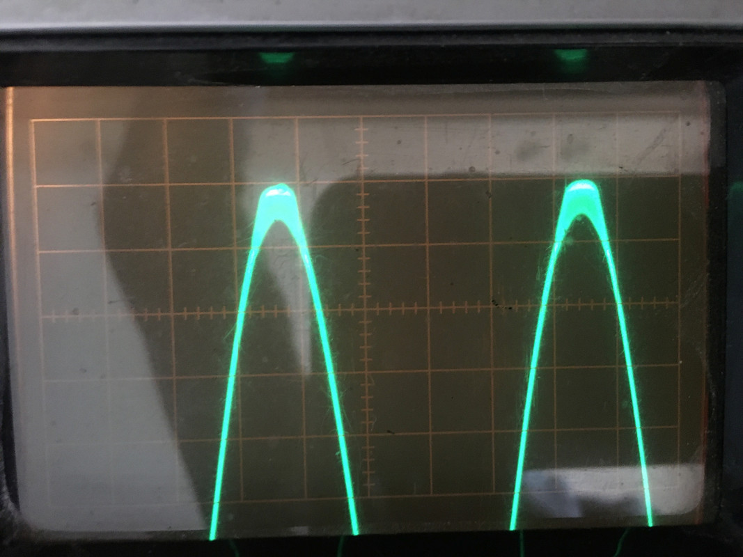
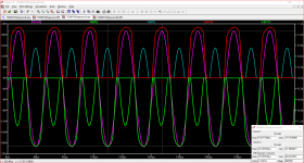
Just to be clear... the oscillation is only on the positive peaks of the sine wave at or near clipping. I don't consider this in any way dangerous to the speakers, especially in normal use. Apologies for my CrApple pictures, the oscillation looks blurred:
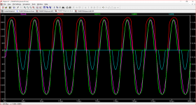
I have run simulations on this circuit. I am attaching a couple of results looking at the emitter currents or the output BJTs and the source and drain currents for the output FETs showing these for peak 20kHz sine outputs at 21V and 34V into 8R.
As the output voltage increases the FETs conduct more and the BJT's conduct less current. The situation reverses when the output voltage is reduced where the FET's conduct less and the BJTs conduct more.
I used Bob Cordell's IRFP9240C and IRFP240C in my simulation for the FETs and other BJTs with supplies of +/- 48.5V.
The zero current cross over voltage point is displaced from zero volts depending the vantage point. I looked at the BJT Output's Ie versus both FET Is and Id in the attached plot images.
I did not take this to the stage of looking at Ig versus Ib however the situation of each half is dynamic in it's own sphere before cross matching with the complementary other half.
It appears that some dynamic aspects can be matched on one side but not for all situations. I don't have any answers on that score however the THD at 20kHz on sine was around 0.1% at the higher voltage level output reducing to 0.03% at the lower simulation test level.
Looking at the shot you posted for sine wave I remember still4given posted some odd images of his amplifier on square wave nonetheless he appeared to be at ease with the sound. Valve amplifiers are not the best in this regard but they still have a large following.
Attachments
Member
Joined 2009
Paid Member
Good work fellas !
There's a lot about this amp I haven't probed or tested. It's good to see the interest here. A bit of oscillation at clipping is not an unusual thing to see in an amplifier - of course it's somewhat undesirable and a bit of work could probably be done to eliminate this behaviour.
I think one suggestion that I made, based on ideas from mjona was to remove the diodes from the gates of the output FETs as their capacitance doesn't help. But a CFP is a bit of an oily pig to control.
Another question was about max power - I never tested for max power, mostly I have found it's too darn loud already using all the speakers I own. But the output swing maybe limited by an overly aggressive RC filter on the power rail to the front end, try reducing the R for more headroom there. Ultimately, MOSFETs do require some room for their gate turn on voltages.
If we wanted to evolve this amp to higher power I'm sure it can be done. A careful consideration of voltage ratings for parts and 60V rails wouldn't be much of a worry.
Hi bigun
I have been reading about this amp and compared it with your tgm1 where you placed a diode in series with r24 100ohms resistor (refering to the schema in post w3).
Here you do not have the diode... what should be the purpose of that component in the v++ rail ?
I have been reading about this amp and compared it with your tgm1 where you placed a diode in series with r24 100ohms resistor (refering to the schema in post w3).
Here you do not have the diode... what should be the purpose of that component in the v++ rail ?
Good work fellas !
There's a lot about this amp I haven't probed or tested. It's good to see the interest here. A bit of oscillation at clipping is not an unusual thing to see in an amplifier - of course it's somewhat undesirable and a bit of work could probably be done to eliminate this behaviour.
I think one suggestion that I made, based on ideas from mjona was to remove the diodes from the gates of the output FETs as their capacitance doesn't help. But a CFP is a bit of an oily pig to control.
Another question was about max power - I never tested for max power, mostly I have found it's too darn loud already using all the speakers I own. But the output swing maybe limited by an overly aggressive RC filter on the power rail to the front end, try reducing the R for more headroom there. Ultimately, MOSFETs do require some room for their gate turn on voltages.
If we wanted to evolve this amp to higher power I'm sure it can be done. A careful consideration of voltage ratings for parts and 60V rails wouldn't be much of a worry.
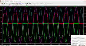
It is possible the dc offset adjust has to be set to satisfy the dc conditions for the FETs since with a BJT complementary stage the lowest current would be a little above the zero voltage level on either side.
If the FETs are not in sych with each other on the time scale - there being some microsecond delay between the hand over - this is much less good than the delay with the handover between the BJTs.
FETs might be faster in theory but is due to capability well beyond audio frequencies so if these are idling away for too long, the thickening of the sine wave shown by Dave S seems to support a combination of two sources following one on the heels after another -this rather than one exactly overlaying the other.
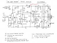
Back in 1980 Linsley-Hood designed a power amplifier using a form of triple output using Darlington Monolith Power Transistors in a more straightforward CFP arrangement. Later he replaced these with Hitachi MOSFETs.
Hi bigun
I have been reading about this amp and compared it with your tgm1 where you placed a diode in series with r24 100ohms resistor (refering to the schema in post w3).
Here you do not have the diode... what should be the purpose of that component in the v++ rail ?
Attachments
Member
Joined 2009
Paid Member
Hi RC,
The main reason that I used this diode was to be faithful to the original design which is the AKSA amplifier. I remember reading about this diode in other bootstrap designs and it’s purpose is linked to the bootstrap current source used for the VA; the diode gives the bootstrap something to ‘push against’ in the positive rail and protects the front end of the amplifier from those tomes when the output stage pulls the positive rail down during heavy current draw. More importantly, Hugh said it did allow the bootstrap to create a little second harmonic; there are other important mechanisms in that design for creating second harmonics but they all work together. In TGM8 I didn’t feel this diode was needed.
The main reason that I used this diode was to be faithful to the original design which is the AKSA amplifier. I remember reading about this diode in other bootstrap designs and it’s purpose is linked to the bootstrap current source used for the VA; the diode gives the bootstrap something to ‘push against’ in the positive rail and protects the front end of the amplifier from those tomes when the output stage pulls the positive rail down during heavy current draw. More importantly, Hugh said it did allow the bootstrap to create a little second harmonic; there are other important mechanisms in that design for creating second harmonics but they all work together. In TGM8 I didn’t feel this diode was needed.
Last edited:
Hi RC,
The main reason that I used this diode was to be faithful to the original design which is the AKSA amplifier. I remember reading about this diode in other bootstrap designs and it’s purpose is linked to the bootstrap current source used for the VA; the diode gives the bootstrap something to ‘push against’ in the positive rail and protects the front end of the amplifier from those tomes when the output stage pulls the positive rail down during heavy current draw. More importantly, Hugh said it did allow the bootstrap to create a little second harmonic; there are other important mechanisms in that design for creating second harmonics but they all work together. In TGM8 I didn’t feel this diode was needed.
Thank you....
I am wondering why I keep seeing these diodes in high power amps even if there are no bootstraps evident like here:
Attachments
Last edited:
Member
Joined 2009
Paid Member
I note that they have diodes on both rails. I would guess it is more than avoiding the output stage causing power rail 'sag', it may also be to protect for other issues, whether power-up, power down sequencing and ensuring discharging caps don't hard things, and with clamp diodes on the output to protect the output stage from speaker back emf there maybe a need to protect the front end too. I've never looked at the details of really high power amps. There's something to learn from those designers.
I note that they have diodes on both rails. I would guess it is more than avoiding the output stage causing power rail 'sag', it may also be to protect for other issues, whether power-up, power down sequencing and ensuring discharging caps don't hard things, and with clamp diodes on the output to protect the output stage from speaker back emf there maybe a need to protect the front end too. I've never looked at the details of really high power amps. There's something to learn from those designers.
Thank you so much for your input.... in fact I am now building another TGM8 based amp and wanted to know if those diodes could somehow filter the rails between the output stage and the input stage...
My memory is not clear on this but there was an article published in Wireless World which could have been after the name change to Electronics and Wireless World about switching effects in Class B output stages generating a spray of harmonics in general and these would be expressed on the supply rails. This might have been due to Anthony Holton referred to in post 1087.
The commonly held view is that current flows from collector to emitter and therefore a diode is necessary in the positive rail as per the example in the attachment to post 1087.
On the other hand BJT carrier charges flow in the opposite direction to current so the attention to stopping ripple entering the voltage gain stages is to do so where emitters are connected to a voltage supply rail.
In the AKSA based circuit the LTP transistor emitters are connected to the positive rail while the general philosophy of the design seems to be to avoid CCS structures and use a simple approach using a resistor there and to bootstrap the collector load on the VAS transistor.
In contrast a Blameless style of amplifier would use CCS structures and current mirrors and an RC filter in the rail feeding the emitters in the stages preceding the outputs. The R element would be kept low and that for C would be larger to compensate.
One could always set up a separate rectifier bridge capacitor supply to feed the stages up to the VAS. This approach was used in a 330W Rotel amplifier dual mono running off 70volt supplies.
The stages including the drivers used 6800uF for the C element of the bridge rectification while the output rectification used 2200uF. The energy in joules of a high voltage supply is given by (Q*V^2) /2.
In principle the charging pulses for 2200uF will produce less supply ripple since the charging time will be shorter than with 10,000uF.
There is a propensity to go large with supply capacitors which take up a lot of internal in space in a box.
One can do the maths to see what might be possible to mitigate against ripple in the Rotel approach. The model involved is rhb10 - a service manual showing circuit detail is available from Hi-Fi Engine.
Last edited:
Board photos
Could any of you that are able/willing to please post close ups of your working finished boards please? I've already seen one or two photos from Gareth's build but as it has taken me so long to get to the point of finally starting my build, I wanted to minimise any build errors and increase the chances of it working! 🙂
Many thanks.
Another possible Approach?
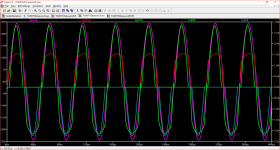
My memory is not what it used to be having forgotten about some correspondence I had with Gareth about this circuit and I have found a simulation I did at the time.
Anyway I have run this and compared the detail with the images attached to my post 1081 which represent the circuit with the output BJT and FET having exchanged places in each output half.
I did not post the .asc file at the time as I was not proposing to built the amplifier in any form as there comes a time when there are just too many projects taking up space in the den. That situation remains unchanged.
The new images show equal current sharing between the BJTs and FETs and the alignment is time is virtually uniform. The simulated 20kHz THD is also better at <0.02% 36V peak into 8R.
Attachments

Member
Joined 2009
Paid Member
Could any of you that are able/willing to please post close ups of your working finished boards please? I've already seen one or two photos from Gareth's build but as it has taken me so long to get to the point of finally starting my build, I wanted to minimise any build errors and increase the chances of it working! 🙂
Many thanks.
I find it helpful to print a hardcopy, scaled to full page size, of the pcb design showing the components without all the tracks etc. I also print a hardcopy of the BOM with additional columns added. I have a column for “kitted” and “installed”. Then I kit all the parts, ticking them off as I go. In a similar fashion I tick off the parts as they are installed on the board and also use a highlight marker pen to colour them off on the printed copy of the pcb design. There are images of the pcb somewhere in this thread but if you download the pcb design files (the software has a free version you can download) then you can create whatever printed guides you want.
Iansmusical, see post #949 for top and bottom images of the pcb that I made to help with building the pcb. I printed these out to use to locate and place parts.
George
George

Hi bigun
I have another question for you...
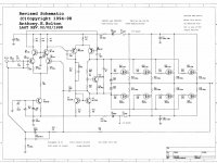
Regarding the schematic in post 60, i see r10 (470k ohm) and i would like to have a clearer idea of its purpose... you state it is optional... can i leave it out even if using clead cap (c5) ?
I have another question for you...
Regarding the schematic in post 60, i see r10 (470k ohm) and i would like to have a clearer idea of its purpose... you state it is optional... can i leave it out even if using clead cap (c5) ?
Member
Joined 2009
Paid Member
Hi RC,
Hey! good question and yes this is an interesting resistor, it provides for some additional feedback directly from the output of the VAS. The reason it is shown as optional is that it is not required for stability, neither is it required for the lowest distortion. It is a little “spice for taste”. This nested feedback was first recommended to me by Hugh dean who used it in his famous AKSA amplifier, where he said it improved the subjective sound quality. It is a fast feedback loop with less phase shift than feedback derived from the output stage, so it will behave differently than feedback only from the output stage. This amplifier is a fairly high feedback-factor amplifier so it may be less sensitive to a touch of nested feedback unless the nested feedback is quite substantial, resulting in less feedback from the output stage. I can’t guide you on what to do but it could be very interesting to play with the balance of feedback between local and global - I haven’t tested it this way however I can confirm that you can leave out this resistor.
Hey! good question and yes this is an interesting resistor, it provides for some additional feedback directly from the output of the VAS. The reason it is shown as optional is that it is not required for stability, neither is it required for the lowest distortion. It is a little “spice for taste”. This nested feedback was first recommended to me by Hugh dean who used it in his famous AKSA amplifier, where he said it improved the subjective sound quality. It is a fast feedback loop with less phase shift than feedback derived from the output stage, so it will behave differently than feedback only from the output stage. This amplifier is a fairly high feedback-factor amplifier so it may be less sensitive to a touch of nested feedback unless the nested feedback is quite substantial, resulting in less feedback from the output stage. I can’t guide you on what to do but it could be very interesting to play with the balance of feedback between local and global - I haven’t tested it this way however I can confirm that you can leave out this resistor.
Last edited:
Hi bigun
So c5 (clead) performs the same function but at higher frequencies right ?
It provides feedback from the output of the vas at high frequencies... this feedback does not correct the errors of the output stage... it helps phase margin and with it we can reduce cdom... i am not sure if it is the best way to reduce thd at high frequencies... please comment...
As promised:- THD + N for the TGM8 at 2.9V into 10R. Left and right channels:
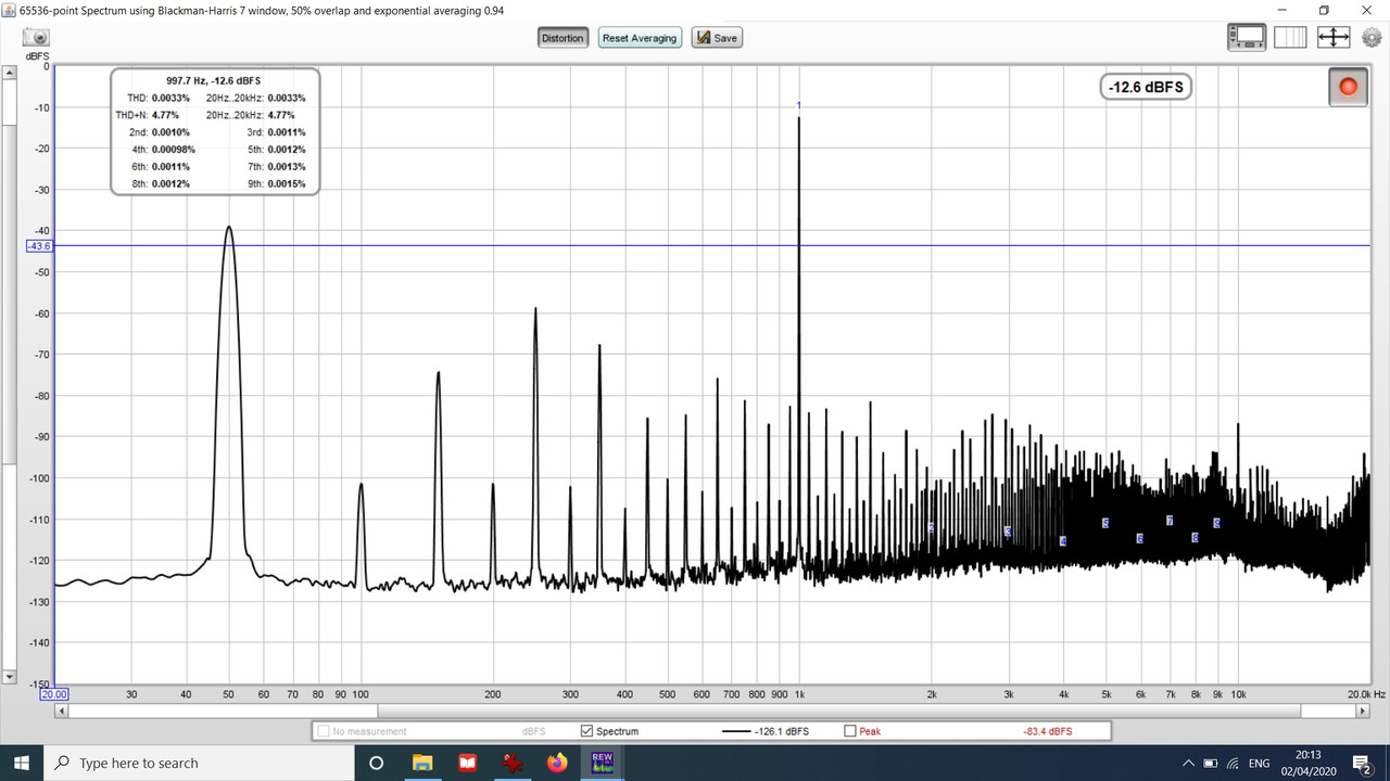
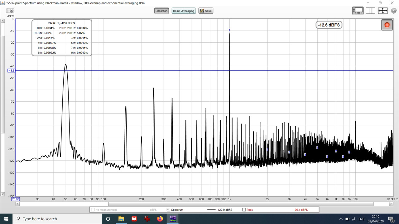
For comparison here are the plots for my Mooly amp (which is a similar design):
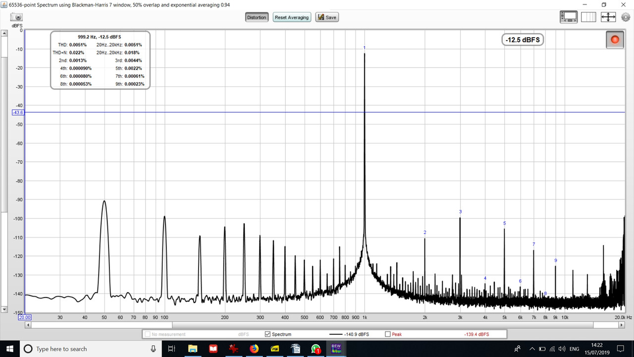
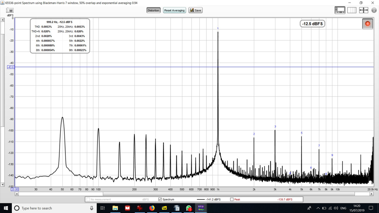
I reckon that the high levels of power supply noise are because of the shared 0V connection for the power transformer centre tap and the speaker 0V.
For comparison here are the plots for my Mooly amp (which is a similar design):
I reckon that the high levels of power supply noise are because of the shared 0V connection for the power transformer centre tap and the speaker 0V.
Hi bigun
I have another question for you...
Regarding the schematic in post 60, i see r10 (470k ohm) and i would like to have a clearer idea of its purpose... you state it is optional... can i leave it out even if using clead cap (c5) ?
The designation of that 470k resistor is now R8.
Looking at a Tian simulation plot with this out of circuit the unity gain bandwidth product is 65 dB - although unusually this increases to 67 dB from 5Hz on up to a few hundred Hz. It gets down to 50dB around 17kHz.
On the other hand with R8 in circuit the level is flat at 50dB from 1Hz up to 5.5kHz.
In both cases the phase at 0dB is -128 degrees leaving a phase margin of 52 degrees.
- Home
- Amplifiers
- Solid State
- TGM8 - my best amplifier, incredible bass, clear highs, no fatigue (inspired by Rod Elliot P3a)