Thx, 10pf it will be.
The 470uF Shunt FB cap (C124 or C7) is a bipolar Muse cap.
I suppose it can also be a 470uF Silmic ?
I already have such silmics.
The 470uF Shunt FB cap (C124 or C7) is a bipolar Muse cap.
I suppose it can also be a 470uF Silmic ?
I already have such silmics.
Hi X,
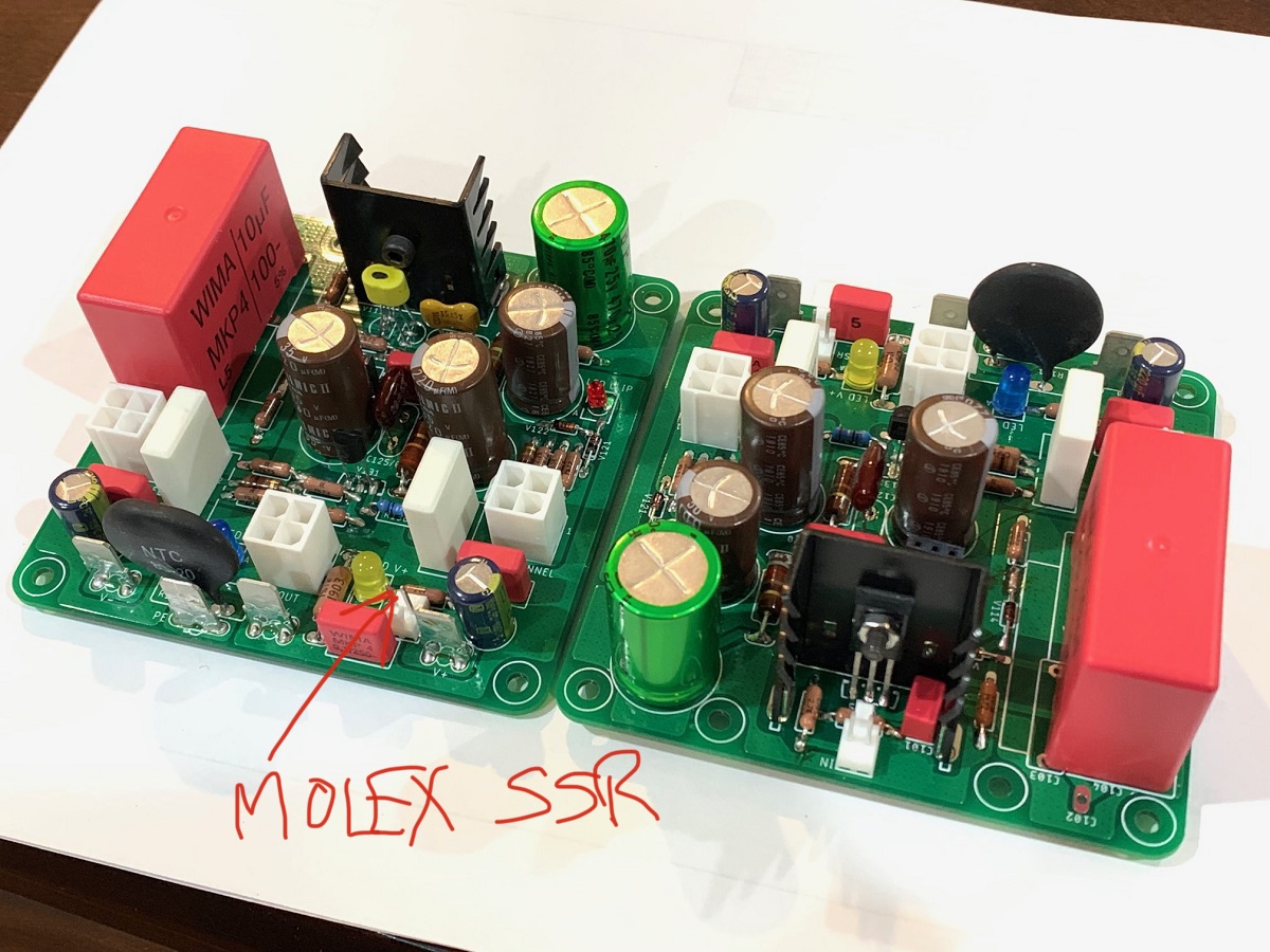
Received the AN pcbs, very nice packaging with the SSR!
Looks like i have to digest this whole thread to see if i should stick with 8 ohm or 4 ohm version.
Received the AN pcbs, very nice packaging with the SSR!
Looks like i have to digest this whole thread to see if i should stick with 8 ohm or 4 ohm version.
I used spades for the speaker connected at the Alpha Nirvana PCB according to this diagram:
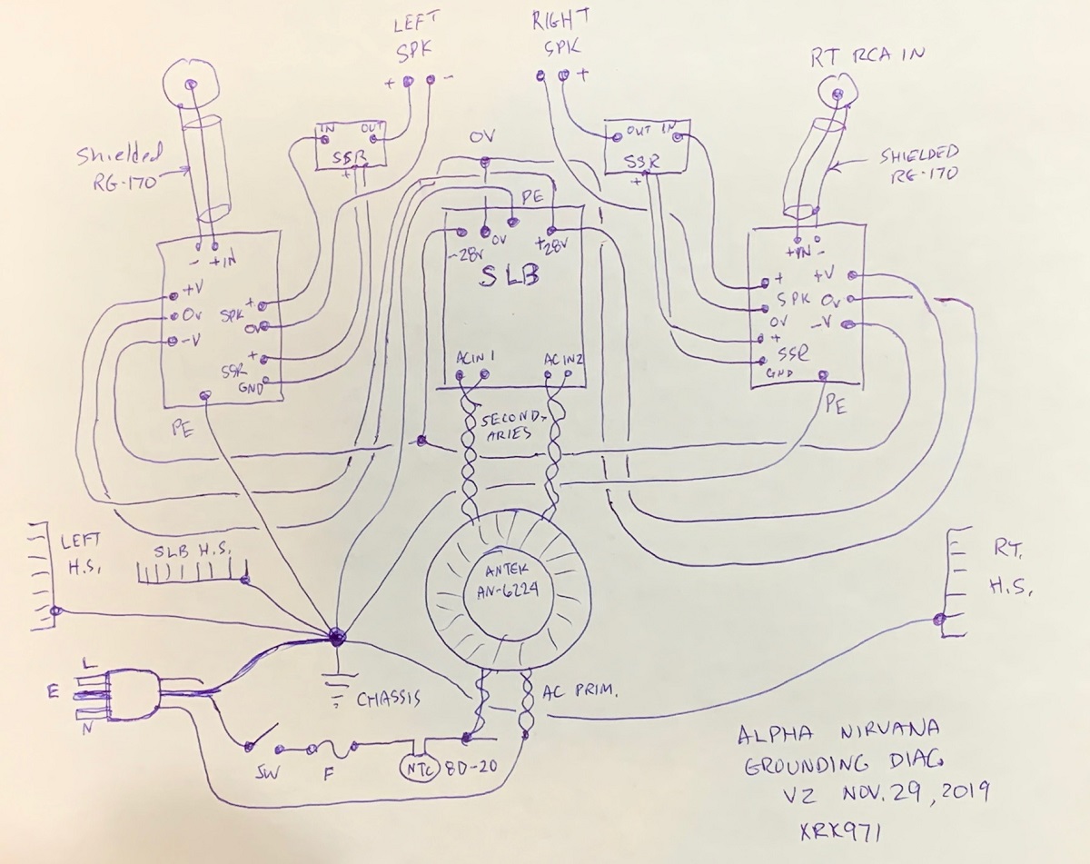
Sorry, X - your diagram doesn't quite show that, to me. 😱
So I have drawn up my own wiring diagram for an AN monobloc - ie:
* 1 power traffo
* 1 SLB
* 1 AN board
* 1 SSR.
What do you think of the attached (sorry for the small size)?
The main difference (apart from drawing spades) is that I took power for the SSR board from the SLB (not the AN board) - given the SLB has multiple spades for GND and two spades for +ve V ... whereas the AN board doesn't.
Andy
Attachments
The AN has a special 2pin Molex KK called SSR specifically to give you power for the SSR. Don’t need to use any of the spades for 4mA of +ve rail current.

I think you are right, I used spades for the power but the 4pin Molex for the speaker out.
I think you are right, I used spades for the power but the 4pin Molex for the speaker out.
Attachments

Last edited:
The AN has a special 2pin Molex KK called SSR specifically to give you power for the SSR. Don’t need to use any of the spades for 4mA of +ve rail current.
Aah, thanks, X - spotted it. Excellent!
I will modify my monobloc wiring daigram and re-post.
Andy
Looks like i have to digest this whole thread to see if i should stick with 8 ohm or 4 ohm version.
Surely it's quite simple?
1. if your spkrs are a difficult load to drive - ie. their impedance drops to 4 ohms (or even below) - then you need the 4R version.
2. otoh, if they are an easy load - then the 8R version is the one to go for, because that is able to deliver more power.
Andy
The AN has a special 2pin Molex KK called SSR specifically to give you power for the SSR.
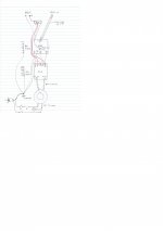
Here is my corrected monobloc AN wiring diagram.
Andy
Attachments
Last edited:
Hi meanie,Looks like i have to digest this whole thread to see if i should stick with 8 ohm or 4 ohm version.
The 4R version is when you need 4R at large voltage swing, that is 4R speakers with low sensitivity.
But for my 4R 93db speakers I usually listen at 1-2vpp, so the 8R will do for me,
X did the calculation.
Danny
Via stitching
I've been starting to learn about the basics of PCB design, and I'm curious about the relationship between impedance between two points and the number of vias stitching parallel top and bottom traces together. I've done some searching but haven't found any explanation of JPS's methodology, and I haven't seen anyone else stitch the same way. I've read about and understand how vias work in general for stitching and shielding, but I haven't seen an explanation for the use of such dense via placement.
The math for calculating cross-sectional area of a trace is straightforward with the size of the via hole and the via plating thickness, and it seems like such dense placement of vias actually decreases the amount of conductive material between two points. Especially when through-hole components are involved, it would seem preferable to prioritize the cross sectional area of the traces, since there will be hardly any voltage gradient between the traces which will push current across the vias, as each trace on each side has a direct connection to the through-hole component. If the top and bottom are truly parallel, then it would seem as if the trace itself is the primary conductor, and not the vias, since there is usually more conductor in the trace than in the vias, so that the trace is a lower impedance path to the second point than going through the vias and the other trace. However, if cross-sectional area is not the goal, though, I'm curious what other effect the vias have to lower impedance.
I can understand that when SMD components are involved, they obviously only directly attach to one side, so vias play a much bigger role in carrying current to the other side of the board. Still, I'm unsure about the quantity of vias.
I also understand that impedance is different than resistance, so it may just be more complex than my simple question recognizes.
Is the effect on inductance or capacitance the major difference I'm not considering?
This question of course sets aside the thermal benefits, since sides of the PCB will almost always be at different temperatures.
The layout is designed by JPS64 (a professional with 30 years of experience making mission critical aerospace circuits and audio circuit layouts - more than anyone else I know - so he does indeed understand wire or trace thickness vs current requirements and low frequency vs high freq layout practices). JPS64’s signature designs use double conducting traces stitched with numerous vias - the approach has seemed to work pretty successfully to provide a low inductance, low impedance path for audio signals in numerous amp projects that have been presented here on DIYA.
I've been starting to learn about the basics of PCB design, and I'm curious about the relationship between impedance between two points and the number of vias stitching parallel top and bottom traces together. I've done some searching but haven't found any explanation of JPS's methodology, and I haven't seen anyone else stitch the same way. I've read about and understand how vias work in general for stitching and shielding, but I haven't seen an explanation for the use of such dense via placement.
The math for calculating cross-sectional area of a trace is straightforward with the size of the via hole and the via plating thickness, and it seems like such dense placement of vias actually decreases the amount of conductive material between two points. Especially when through-hole components are involved, it would seem preferable to prioritize the cross sectional area of the traces, since there will be hardly any voltage gradient between the traces which will push current across the vias, as each trace on each side has a direct connection to the through-hole component. If the top and bottom are truly parallel, then it would seem as if the trace itself is the primary conductor, and not the vias, since there is usually more conductor in the trace than in the vias, so that the trace is a lower impedance path to the second point than going through the vias and the other trace. However, if cross-sectional area is not the goal, though, I'm curious what other effect the vias have to lower impedance.
I can understand that when SMD components are involved, they obviously only directly attach to one side, so vias play a much bigger role in carrying current to the other side of the board. Still, I'm unsure about the quantity of vias.
I also understand that impedance is different than resistance, so it may just be more complex than my simple question recognizes.
Is the effect on inductance or capacitance the major difference I'm not considering?
This question of course sets aside the thermal benefits, since sides of the PCB will almost always be at different temperatures.
I think of it like conductive metal “foam” covered by two sheets vs metal sheets alone in conduction. There is more metal with the dense stitching.
I have not looked at the equations. I bet this is something a FEA model in Ansys could tell us right away.
I have not looked at the equations. I bet this is something a FEA model in Ansys could tell us right away.
I think of it like conductive metal “foam” covered by two sheets vs metal sheets alone in conduction. There is more metal with the dense stitching.
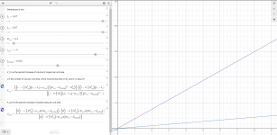
There is more metal in total. While the in-plane cross-section at many points shrinks (e.g., aligned with a row of vias, the only copper in-plane is that passing between the vias, plus the plating on the boundaries), the overall conductor volume increases slightly and the surface area increases substantially. See attached Desmos screenshot.
Perhaps this foam or mesh structure takes advantage of the increased surface area, reducing the impedance for AC signals due to the skin effect? But that wouldn't seem to have significant effects at audio frequencies.
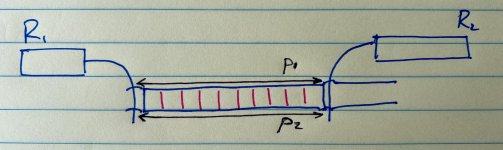
That still leaves me wondering what phenomenon drives current through the vias (below, pink) when the upper and lower traces are the shortest paths, respectively, between through-hole components.
Attachments
Last edited:
Regarding question of what drives current through vias: nothing unless the flow hits a bottleneck on one side or the other. The copper planes are not 100% symmetric on both sides. Sometimes one side is wider in certain places. The vias allow the current to shift sides. Certainly heat transfer is better with the porous boards.
I don’t know - FEA will tell us immediately. In fact, a simple analysis with heat transfer and the Fourier equation will work as well. I recall an undergraduate analog experiment. We cut up sheets of graphite with holes and patterns. Apply voltage along a boundary edge and sink along another boundary. Then take DVM probe and touch points on a grid. We could make contour plots of the equivalent thermal distribution due to conduction. I think from standpoint of an amp it’s probably not a big deal. But it has 3 physical benefits.
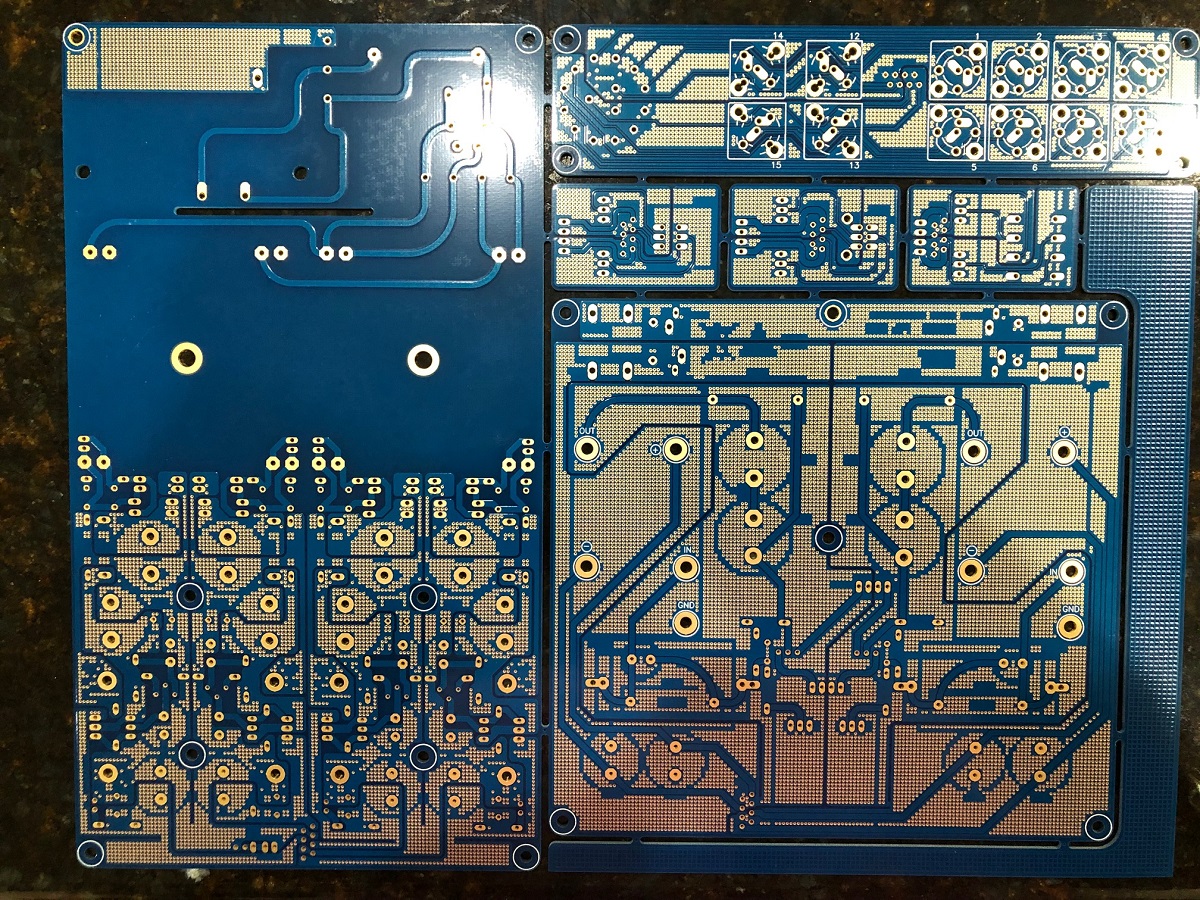
Here is Yarra before we did tented vias mask:
1. The traces are more robust and won’t peel off as easily.
2. The thermal radiation and convective cooling is better.
3. It looks way cool. Especially in gold and no mask.
What is crazy is that there is no extra charge for those 45,000 drill operations and all the extra copper and gold in those holes. 🙂
I don’t know - FEA will tell us immediately. In fact, a simple analysis with heat transfer and the Fourier equation will work as well. I recall an undergraduate analog experiment. We cut up sheets of graphite with holes and patterns. Apply voltage along a boundary edge and sink along another boundary. Then take DVM probe and touch points on a grid. We could make contour plots of the equivalent thermal distribution due to conduction. I think from standpoint of an amp it’s probably not a big deal. But it has 3 physical benefits.
Here is Yarra before we did tented vias mask:
1. The traces are more robust and won’t peel off as easily.
2. The thermal radiation and convective cooling is better.
3. It looks way cool. Especially in gold and no mask.
What is crazy is that there is no extra charge for those 45,000 drill operations and all the extra copper and gold in those holes. 🙂
Last edited:
What is crazy is that there is no extra charge for those 45,000 drill operations and all the extra copper and gold in those holes. 🙂
As long as others don't catch on and start submitting all their orders like this, hopefully it stays that way!
Fortunately, it’s not easy to put all those vias in. They are done by hand in software. There is no “paint my copper traces with vias” button.
Fortunately, it’s not easy to put all those vias in.
Putting them in is easy compared to taking them out after you decide to change the schematic and shuffle the layout. At least in KiCad, I haven't found a "select all vias but not all the components interspersed between" tool.
I have since learned to do vias last - and save a non-stitched version for later revisions.
Last edited:
The AN has a special 2pin Molex KK called SSR specifically to give you power for the SSR. Don’t need to use any of the spades for 4mA of +ve rail current.
Hi X,
Your comment that you "don’t need to use spades for 4mA of current " has raised a niggling thought in my mind. 🙁
Sure those Molex pins are absolutely appropriate for the small currents involved in:
* LED connections
* SSR connections, and
* signal in connections.
You have also used Molex connectors for the AN 8R PCB & SLB PCB - where about 1.7a will be passed:
* to the SLB off-board transistors
* to the AN MOSFETs, and
* to the spkr terminals.
I'm assuming 1.7a is coped with, fine - but in the case of the 4R version, we're talking about 3+ amps going to these off-board devices!
Are you sure the pins & pin-sockets will pass this much current OK?
I'm thinking 3 spades might be more appropriate for each of the off-board connections, instead of Molex connectors? (Doesn't look as sexy - but maybe 'works' better!)
Andy
Andy,
The Molex connectors handle 9A, 600v Max.
I think there is plenty of wiggle room here 😉
https://www.mouser.com/datasheet/2/276/0039281043_PCB_HEADERS-1530237.pdf
The Molex connectors handle 9A, 600v Max.
I think there is plenty of wiggle room here 😉
https://www.mouser.com/datasheet/2/276/0039281043_PCB_HEADERS-1530237.pdf
Andy,
The Molex connectors handle 9A, 600v Max.
I think there is plenty of wiggle room here 😉
https://www.mouser.com/datasheet/2/276/0039281043_PCB_HEADERS-1530237.pdf
Aah, cool - thanks, Vunce. 🙂
I note that the specs say "30 mating cycles, max " - so it's not a good idea to keep plugging & unplugging these connectors!
Andy
Yes Andy, once the amp is assembled tested and working, then there is no need to keep unplugging them.
If it ain't broke - don't fix it I say.
Keep up the good work.
If it ain't broke - don't fix it I say.
Keep up the good work.
Looking for some help.
In the Mouser "Shopping Cart for BOM " link on the first post of this thread, the 3rd item is Wurth Male 4-pin sockets.
The part nos written against this item are:
* X411-3, and
* X1001-2.
But I can't find these part numbers on the "As Built" cct diagram - or the "Top Side View" diagram?
What I can find on the "Top Side View" diagram (which lists all the part numbers) is:
* X141,
* X142, and
* X143
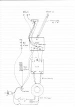
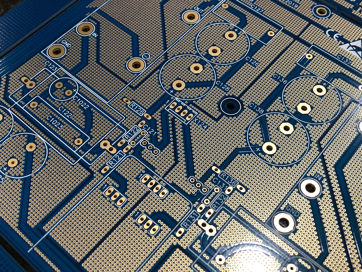
... which are shown in X's pics of his finished boards (attached).
I assume that 'X411-3' is therefore an error and should read X141, X142, X143?
And X1002 is the same unit on the Snubber boards?
Thanks,
Andy

In the Mouser "Shopping Cart for BOM " link on the first post of this thread, the 3rd item is Wurth Male 4-pin sockets.
The part nos written against this item are:
* X411-3, and
* X1001-2.
But I can't find these part numbers on the "As Built" cct diagram - or the "Top Side View" diagram?
What I can find on the "Top Side View" diagram (which lists all the part numbers) is:
* X141,
* X142, and
* X143
... which are shown in X's pics of his finished boards (attached).
I assume that 'X411-3' is therefore an error and should read X141, X142, X143?
And X1002 is the same unit on the Snubber boards?
Thanks,
Andy
Last edited:
- Home
- Amplifiers
- Solid State
- Alpha Nirvana 39w 8ohm Class A Amp