I understood that the Miller Plateau was a MOSFET phenomenon. Or am I missing something obvious about JFETs?
Well, my google-fu is strong. And I fail to find anything like this effect with anything other than nanowire fets at cryogenic temperatures, mesfets, vertical channel fets - and of course MOSFETS.
So if you have any references or links to this effect, whatever it is called, in regular audio jfets like the j170/k74 or similar, that would be good. In other words, in non-exotic structures.
So if you have any references or links to this effect, whatever it is called, in regular audio jfets like the j170/k74 or similar, that would be good. In other words, in non-exotic structures.
The art of electronics-3rd edition page 166/167So if you have any references or links to this effect, whatever it is called, in regular audio jfets like the j170/k74 or similar, that would be good. In other words, in non-exotic structures.
nope...it iis about j-fets and they also discuss on 2n5457 /58 plots...The whole chapter 3 is about j-fets...Which is all about MOSFETS.
Well fine - you want me to look at other pages - OK. But you initially quoted two pages that do not mention JFET's at all. Certainly in my 1998 edition
Third edition...2015Well fine - you want me to look at other pages - OK. But you initially quoted two pages that do not mention JFET's at all. Certainly in my 1998 edition
PM your email address , please!Well fine - you want me to look at other pages - OK. But you initially quoted two pages that do not mention JFET's at all. Certainly in my 1998 edition
Well having had a look through the chapter, of course there is an effect for very low drain currents - it is just the regular k.exp(V/Vt) sort of relationship that is common to any diode-like behaviour - whether it is gate-source junction (whether MOS or J) a base emitter junction or a diode. For FET's it is called the subthreshold region, but it is nothing mysterious.
This is incorporated into the Ebers-Moll spice models of any device.
I might sound a bit pernickety having now understood what you are talking about. But my early research life was in laser development, and a laser pulse builds up exponentially initially from random photon noise until it reaches lasing threshold when there is a total gain of ~e^30.
Why are we discussing this?

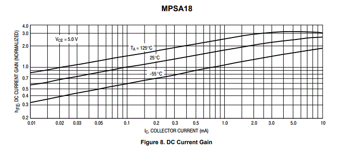
Someone mentioned the mpsa18 in this thread, and Mark's data about quasi-saturation - that is not an issue for me, as I will run them well below 10mA, if I use them for my I/V converter (yet another one).
My question is about the hfe. Is there a purpose to the slope in the hfe x Ic curve? Is the slope intentional, or just a byproduct of the proccess (which has high hfe)?
edit: is that slope useful?
Thanks
Alex
My question is about the hfe. Is there a purpose to the slope in the hfe x Ic curve? Is the slope intentional, or just a byproduct of the proccess (which has high hfe)?
edit: is that slope useful?
Thanks
Alex
Attachments
Last edited:
I'm no device physicist, but the hFE roll-off at low currents is just due to non-idealities, irregularities in the crystal lattice and that sort of thing. In fact the non-ideal base current that causes the roll-off usually has a substantial amount of 1/f noise associated with it, so transistors with less hFE roll-off are likely to have less 1/f noise.
It is a result of recombination in the base emitter junction, and is more a question of the device geometry, carrier mobility and doping profiles rather than lattice imperfections.
The effect continues rolling downwards at the same slope down to pico-amp Ic.
Notice that although there is a clear effect with temperature, the slope is a constant.
The effect continues rolling downwards at the same slope down to pico-amp Ic.
Notice that although there is a clear effect with temperature, the slope is a constant.
If it is not related to defects, why does it get better with thermal annealing and worse when the transistor is subjected to emitter-base avalanche breakdown?
I was misinterpreting the factor DpB in the equations which is the impurity concentration in the base.
I've been looking at a lot of datasheets, trying to figure out some of the intricacies of different types of BJTs and different processes. Here is some data that stands out. These look like perfect complementary pairs under 20mA and have excellent specs, but high beta is not available. One of my suppliers has the E grade in stock.
Attachments
Some articles from one of the authors of the book (Norman H. Crowhurst):
www.audiofaidate.org • Leggi argomento - Crowhurst collection
www.audiofaidate.org • Leggi argomento - Crowhurst collection
- Home
- Source & Line
- Analogue Source
- BC550 BC560 Very low noise RIAA