In post 9 did I show a PCB design, but to make that, do the tracks have to go in all sorts of directions and do get fairly long. But how would that effect the amplifier? I think I have heard several times that traces have to be as short as possible, but what if the traces is wider?
Get all the components laid out so ones that are connected to each other and close to each other.
Then click on "optimise net" and you shouldnt be too far away.
You can think about star grounding later once its routed.
My software also does a "swap autoplace" function which swaps around components for shortest net.
Thanks it's a great advice, my "problem" is that it looks like they all are connected in a fashion, if i put the close together.
Swap components, what a great function, what software do you use? Can KiCad do that?
Swap components, what a great function, what software do you use? Can KiCad do that?
Thanks it's a great advice, my "problem" is that it looks like they all are connected in a fashion, if i put the close together.
Swap components, what a great function, what software do you use? Can KiCad do that?
I tend to put small signal stuff together and away from big signals that might interfere.
I don't think KICAD does "swap auto-placing."
I wrote PCBCAD51 myself and just added what I thought were good "extra" functions as required.
I did a huge digital pcb many years ago that wouldn't route.
So I came up with the "swap auto place" function and that fixed it.

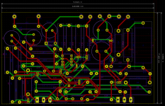
The problems now are tracks touching some pads as they pass by them.
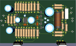
The 3 legged components in the middle of the pcb have pads touching.
The 3 legged components in the middle of the pcb have pads touching.
Okay thanks, that have to be fixed!
But what about these long traces, crossing many components?
All you can do is improve it best you can.
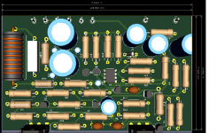
Thanks to your advice about swapping, using FreeRouting and lot other, have I tried to make a board where I totally ignores how it looks, only thinking of minimizing vias and track length.
How it functions is more important.
There are still a few components that look like they have pads shorting.
That means sorting out the libraries.
No not at all, I have just no idea on what I am doing at all, I have no idea on where to start, what to look fore or... anything!
What's the circuit looking like? Maybe just for fun to do some manipulation with what I learned many years ago with the cad program. Some weekend-challange!
Urgghhh... Sorry Mooly, that's not my taste of topology.
Dressing a nest of uglies to suit a moderate flat is always a nice puzzle. But here no added value for me. Sorry again.
Dressing a nest of uglies to suit a moderate flat is always a nice puzzle. But here no added value for me. Sorry again.
....I have absolutely now idea on what I am doing ....connected in a random order....
Then learn from the people who have gone down this road before. Find a dozen or a hundred laid-out amplifier boards and get a sense of what looks good and works good.
They do not have to be the same basic amplifier, because all audio amplifiers have similarities.There's big power devices and little control devices. In a chip-amp they are all in one, but even then the wiring divides into big and little currents. And there are many discrete (or discrete+IC) amplifiers around.
You have the internet. Use It! Back when I got started we could only find about one design a month to study. (Which did mean I had some of them memorized.)
- Home
- Design & Build
- Construction Tips
- Worst PCB track-layout ever?