I found the problem: I had actually missed three vias. Problem fixed, and all vias start from the top and end at the bottom.
Thanks!
And just to make sure, I am using the following 6-layer stack:
1. Signal
2. Ground
3. VCC
4. +3.3V
5. Ground
6. Signal
The only alternatives that I can think of are:
1. Signal
2. Ground
3. +3.3V
4. VCC
5. Ground
6. Signal
Not sure if that makes any difference. And if any, it must be minimal.
1. Signal
2. +3.3V
3. Ground
4. Ground
5. VCC
6. Signal
But losing the ground planes behind signal and power does not seem like a good idea.
Please correct me if I'm wrong, or if I overlooked a better alternative.
Looks fine to me, you can also do polygon pours on top and bottom to connect empty area to ground and then add vias to stitch them. Altium has a via stitching tool that automates it for you, but copy and paste works fine.
Looks fine to me, you can also do polygon pours on top and bottom to connect empty area to ground and then add vias to stitch them. Altium has a via stitching tool that automates it for you, but copy and paste works fine.
Awesome!
Yes, I think I should do that. I tried to do it yesterday for the internal planes, without realizing that Altium does the pour for you once the layer is marked as an internal plane. But for the top and bottom layers, it has to be done manually. I'll give it a shot.
Awesome!
Yes, I think I should do that. I tried to do it yesterday for the internal planes, without realizing that Altium does the pour for you once the layer is marked as an internal plane. But for the top and bottom layers, it has to be done manually. I'll give it a shot.
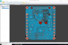
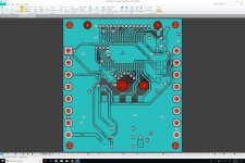
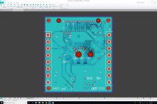
Here are the top and bottom layers with GND pours.
I love it when the software does so much work for free!
Is there anything else you'd change on the board (short of redesigning everything from scratch)?
Please do not hesitate to be critical — I'm here to learn.
Attachments
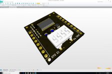
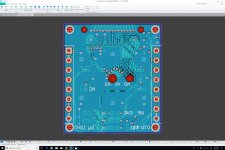
Black Solder Mask
Here is the PCB with black solder mask, because for musicians, black is the way to go. We will use black for the bricks and blocks (the 3 × 3 mikroBUS on which bricks will be mounted), while using white for the trays (the 2 × 3 USB grids on which blocks will be mounted).
We've also selected the "Top-Middle-Bottom" Size and Shape option for the four through-holes that will be used with the M1.2 screws. This allowed us to remove the copper pads on the bottom layer, thereby avoiding any interference with the overlay outline for the mikroBUS headers. This is a tiny cosmetic detail, but we're trying to develop a better understanding for all these aspects, ahead of a more complex project (the DAC board).
And we've added overlay marking for the I²C address selector.
Last but not least, we've switched back to the standard Stroke font for overlay markings, instead of using the Roboto Mono True Type font. This should improve readability and avoid any problems with a font that was certainly not designed for PCB overlays. We're still using Roboto Mono for labels within Altium CircuitStudio, because it's a lot cleaner than the Times New Roman Serif font that is used by default (what a bizarre default setting).
And did I mention that I am really impressed by Altium's 3D rendering? I would pay for the software just for the quality of that feature. When compared to what one has to do to generate a 3D rendering using Autodesk Eagle, this is night and day! I just wish that I could make it work with my 3Dconnexion SpaceMouse (somehow it's not recognized by the software).
Attachments
Last edited:
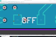
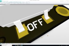
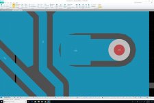
The "OFF" overlay marking for the voltage selector is printed on top of a via. Is that considered bad practice?
Just to be on the safe side, we moved the via, which will also make the display of the OFF marking a tiny bit cleaner.
Attachments
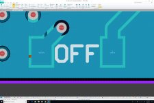
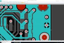
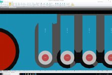
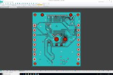
Multiple Vias for same trace
On some long traces that need a via, we sometimes add additional vias. For example, on VCC, we had only one at the top right of the trace, but we decided to add a second one at the bottom in the middle. I am assuming this is okay. Please let me know otherwise.
On some long traces that need a via, we sometimes add additional vias. For example, on VCC, we had only one at the top right of the trace, but we decided to add a second one at the bottom in the middle. I am assuming this is okay. Please let me know otherwise.
Attachments
No Logo
As far as I can tell, CircuitStudio does not support the resizing of Unions. As a result, we cannot properly resize any BMP image used for our logo. Therefore, we'll have to settle on a more mundane lettering until we upgrade to Designer.
As far as I can tell, CircuitStudio does not support the resizing of Unions. As a result, we cannot properly resize any BMP image used for our logo. Therefore, we'll have to settle on a more mundane lettering until we upgrade to Designer.
Attachments
Here are the top and bottom layers with GND pours.
I love it when the software does so much work for free!
Is there anything else you'd change on the board (short of redesigning everything from scratch)?
Please do not hesitate to be critical — I'm here to learn.
I would remove thermal reliefs from your vias, in Altium you may have to create PlaneConnect and PolygonConnect rules that specify Direct instead of Relief. I would also remove them on SMT pads if you are going to have it professionally assembled or assembled via reflow soldering.
I would also use multiple vias for any higher current power traces when switching layers and try to get the vias closer to pads for decoupling caps (less trace, less inductance).
See Figure 3 in the link here:
Board Design Resource Center
Got it! So, for capacitors, as thick a trace as possible and vias on the side instead of at the end.
I'll try to remove the thermal reliefs.
Thanks a lot!
I would remove thermal reliefs from your vias, in Altium you may have to create PlaneConnect and PolygonConnect rules that specify Direct instead of Relief. I would also remove them on SMT pads if you are going to have it professionally assembled or assembled via reflow soldering.
I would also use multiple vias for any higher current power traces when switching layers and try to get the vias closer to pads for decoupling caps (less trace, less inductance).
See Figure 3 in the link here:
Board Design Resource Center
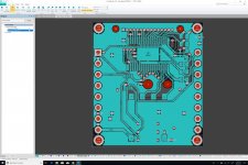
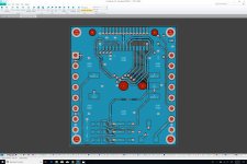
Here is a new version with Direct for both Planes and Polygons. I'll write a separate post with additional questions.
Attachments

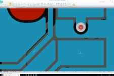
Questions about pours
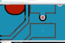
Here are three examples of artifacts that appear with pours, and I am wondering whether they're bad, and whether there is any way to get rid of them.
# Screenshot 1: Long way to via while GND was all around.
# Screenshot 2: Tiny holes in the pour.
# Screenshot 3: GND cul-de-sac.
Here are three examples of artifacts that appear with pours, and I am wondering whether they're bad, and whether there is any way to get rid of them.
# Screenshot 1: Long way to via while GND was all around.
# Screenshot 2: Tiny holes in the pour.
# Screenshot 3: GND cul-de-sac.
Attachments

Last edited:
Surface Mount Nut
Here is the surface mount threaded standoff that we can use for the mezzanine board: SMTSO-M1.4-3-ET. You can see it on page 4 of this catalog. Thankfully, it's available in 3 different lengths (1mm, 2mm, and 3mm), which means that we won't have any problems finding the right pair of screw and standoff. To be perfectly honest, the availability of such a standoff in M1.4 comes as a relief, because without it, the whole design would pretty much fall apart...
Here is the surface mount threaded standoff that we can use for the mezzanine board: SMTSO-M1.4-3-ET. You can see it on page 4 of this catalog. Thankfully, it's available in 3 different lengths (1mm, 2mm, and 3mm), which means that we won't have any problems finding the right pair of screw and standoff. To be perfectly honest, the availability of such a standoff in M1.4 comes as a relief, because without it, the whole design would pretty much fall apart...
Here are three examples of artifacts that appear with pours, and I am wondering whether they're bad, and whether there is any way to get rid of them.
# Screenshot 1: Long way to via while GND was all around.
# Screenshot 2: Tiny holes in the pour.
# Screenshot 3: GND cul-de-sac.
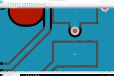
Here is another couple of examples:
# Screenshot 1: GND cul-de-sac.
# Screenshot 2: The two GND pours should be connected.
Attachments
There should be an option for polygons to set them to "pour over all same net objects". I think it's not doing that right now. There might also be an option to remove slivers / dead copper smaller than a certain size. If the area is large enough for a via, then you can put a via in it to make sure it's well connected.
There should be an option for polygons to set them to "pour over all same net objects". I think it's not doing that right now. There might also be an option to remove slivers / dead copper smaller than a certain size. If the area is large enough for a via, then you can put a via in it to make sure it's well connected.
You got it! It worked. Thank you so much...
Attachments
You got it! It worked. Thank you so much...
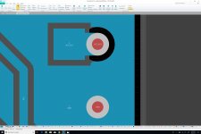
And here is a fix for the two disjointed GND areas. This was achieved by simply moving a trace 10 mil NW.
Attachments
I would remove thermal reliefs from your vias, in Altium you may have to create PlaneConnect and PolygonConnect rules that specify Direct instead of Relief. I would also remove them on SMT pads if you are going to have it professionally assembled or assembled via reflow soldering.
I would also use multiple vias for any higher current power traces when switching layers and try to get the vias closer to pads for decoupling caps (less trace, less inductance).
See Figure 3 in the link here:
Board Design Resource Center
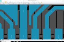
Here is an example of a decoupling cap for which the vias have been brought closer to the cap's pads. And the vias are mounted sideways of course...
Attachments
- Home
- Source & Line
- Digital Line Level
- 8 × AK5578EN + 8 × AK4499EQ ADC/DAC Boards