X - the programmable dual rail supply is only programmable on the positive rail .. neg is fixed -5V
You could go in and reprogram the resistors following the guidance of the datasheet. I have done this when designing my own custom dual rail supplies with these chips.
Look at Table 2 in the following data sheet - trace out on the ebay board where those resistors are and replace them,
http://www.ti.com/lit/ds/symlink/tps7a33.pdf
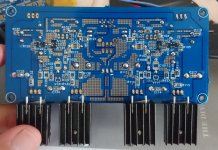
Finished soldering everything and hooked it all up, but only the left channel works, the right channel mosfets feel cold..so something somewhere isn't right.
Just to make sure I have the power wired up correctly - I'm using X113, and pin 1 on the silk screen is negative, middle ground, and right is positive.
Is there any particular place I should start the fault finding?
Just to make sure I have the power wired up correctly - I'm using X113, and pin 1 on the silk screen is negative, middle ground, and right is positive.
Is there any particular place I should start the fault finding?
Last edited:
Do you have any pictures of your board?
Easiest thing is to print a copy of the schematic and get a highlighter. Using a multimeter, follow the circuit from the power supply, checking for correct voltages, comparing both sides until you find a difference, marking off the schematic as you go.
Also follow the input signal left and right channel.
Probably nothing to do with your problem, but did you follow this as well:
Update Aug. 5, 2018: Silkscreen on PSU PCB has error: Diode V241 has cathode and anode flipped.. Mount diode with Anode towards Drain of P channel MOSFET on cap Mx.
Last edited:
The PSU jacks are tied together so if left channel works the right channel should be getting same rails. Yes, left pin 1 is negative and middle pin is GND and right is positive.
Measure your bias current through R116/118 or R117/115. What is output node DC voltage?
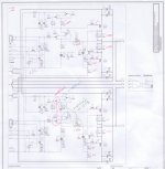
The best way to help us debug is to take a DMM and probe the DC setpoints voltages at all major nodes and pins of actives. Then take a red pen and write those voltages at the correct physical location on the printed out schematic. Then scan or take a photonof that marked up diagnostic schematic and post it. It tells all and will pinpoint the fault.
Couple of general things to try.
1. Touch up all solder joints to reflow them and get rid of cold solder joints. Look at SMT parts. If there is not a visible meniscus or fillet of solder, it’s probably a bad joint.
2. Double check all installed resistor values. Sometimes parts get mispackaged at factory or we make a visual reading mistake and slip a factor of 100 or 1000 ohms.
3. Makes sure all actives are correct. Like you did not accidentally install N channel MOSFETs as all outputs are P channel.
4. Make sure none of the SMT caps are shorted with a solder bridge underneath.
You have one channel working so compare parts from left to right.
Good luck!
Measure your bias current through R116/118 or R117/115. What is output node DC voltage?
The best way to help us debug is to take a DMM and probe the DC setpoints voltages at all major nodes and pins of actives. Then take a red pen and write those voltages at the correct physical location on the printed out schematic. Then scan or take a photonof that marked up diagnostic schematic and post it. It tells all and will pinpoint the fault.
Couple of general things to try.
1. Touch up all solder joints to reflow them and get rid of cold solder joints. Look at SMT parts. If there is not a visible meniscus or fillet of solder, it’s probably a bad joint.
2. Double check all installed resistor values. Sometimes parts get mispackaged at factory or we make a visual reading mistake and slip a factor of 100 or 1000 ohms.
3. Makes sure all actives are correct. Like you did not accidentally install N channel MOSFETs as all outputs are P channel.
4. Make sure none of the SMT caps are shorted with a solder bridge underneath.
You have one channel working so compare parts from left to right.
Good luck!
hmm..that would be a very good starting point 
I'm sure I crossed them off on the BOM though.
Although, how does one channel function without it?
I'm sure I crossed them off on the BOM though.
Although, how does one channel function without it?
Although, how does one channel function without it?
😕 Beats me!
🙂
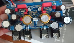
Ok, installed v111 and v131, current draw is now down from 2A @ 15V from bench psu to about half an amp.
now there's sound from right channel, but distorted, and V133 and 134 are still cool to touch as opposed to 113 and 114 which are warm.
Will proceed with checking for shorts & voltages
now there's sound from right channel, but distorted, and V133 and 134 are still cool to touch as opposed to 113 and 114 which are warm.
Will proceed with checking for shorts & voltages
Without the BJT, there won't be any bias voltage across the lower MOSFET and thus, no bias current and no heat.
If there is sound and it is distorted, probably means bias current is still not working. Please measure the current across one the main resistors in the output stage.
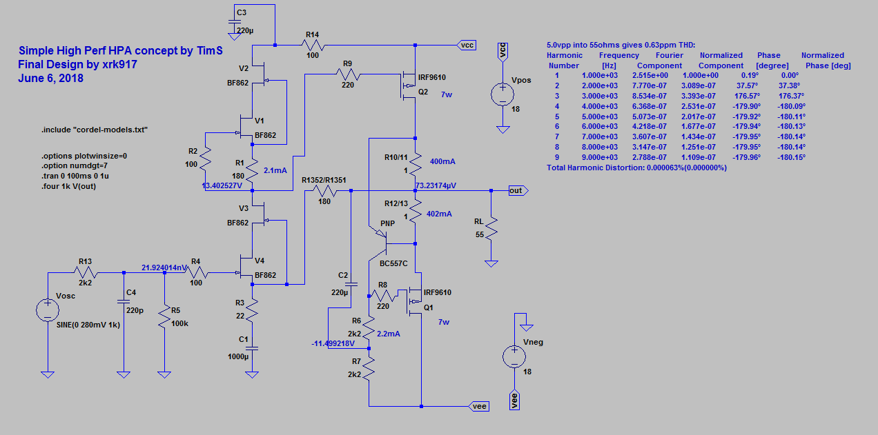
If there is sound and it is distorted, probably means bias current is still not working. Please measure the current across one the main resistors in the output stage.
Here's measurements on the schematic - jfet stages seems to be working - similar voltages on both channels, mosfet stage - left (distorted) channel has 0V at the gate of both mosfets, and across R137 & 138.
Would bad mosfet(s) on the left be the conclusion?
I've also ticked off components against BOM - all seems correct now, I used mostly the through hole WIMAs instead of SMT caps, and there were a few dodgy SMT joints that I touched up as well.
Would bad mosfet(s) on the left be the conclusion?
I've also ticked off components against BOM - all seems correct now, I used mostly the through hole WIMAs instead of SMT caps, and there were a few dodgy SMT joints that I touched up as well.
Attachments
Last edited:
There are only a few ways for the G of V133 to be 0v: a solder bridge on G to ground plane on opposite side, or for MOSFET to be dead (open circuit). As R133 is connected to JFETs which appear to be working, there should be similar voltage to L-channel. Are you certain that those are IRF9610 (P-channel) installed on V133 and V134?
I used FQP3P20 since the BOM said they were the lower distortion sub for the 9610...all 4 came from the same tube, will double check the part numbers are correct & check for shorts
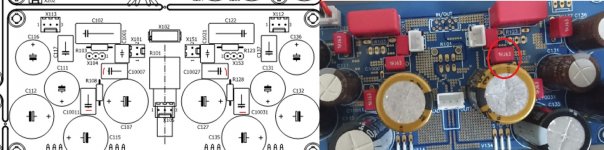
Looks like he using Wima film caps there, so not an issue.Are you using polarised caps for c10007, c10027
Make sure you did not install a BF862 JFET where there should be a BC857 PNP BJT. The BF862 are labeled "AW2" I think. Since both are SOT23, it is easy to mix them up.
So there is something very different between your two channels. Check the bad channel vs the good channel part by part - make sure all resistors are the correct value.
You verified that all installed MOSFETs are indeed P channel? Sometimes they put an N channel in a P channel tube. And we take it out and use it without looking to see if it is the right part.
You verified that all installed MOSFETs are indeed P channel? Sometimes they put an N channel in a P channel tube. And we take it out and use it without looking to see if it is the right part.
part numbers on the package match between all 4 of them, will check parts again, I did it yesterday, but admittedly that was at night while I was tired.
I guess if it all checked out I'll swap the 2 mosfets for the right channel and see
I guess if it all checked out I'll swap the 2 mosfets for the right channel and see
All the resistors are correct values (checked SMD parts based of case marking - didn't measure), MOSFETS on right channel were good - pulled them and tested on those parts testers, confirmed working & P channel.
Swapped them anyway (tested the replacements before soldering them in) - no difference. Touched up all of the right channel solder joints too, and still no difference.
Right MOSFETS are still cold to touch whereas left warm up.
Is there a possibility of a bad BF862 in the right? Or is continuity checking everything the next step before pointing fingers at transistors?
Last edited:
- Home
- Group Buys
- Simple High Performance DC Coupled Class A HPA with sub PPM THD