Of course I agree, but I don't see my results contradict that.
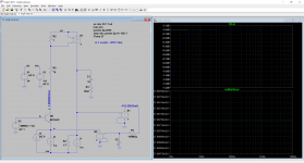
Here are results with almost the same scheme as your.
You can see that for RLOAD = 250kohm (R cancellation/2) ic/vbe is also near 0.
This Ro cancellation is not devoid of collateral damage.
Would you mind verifying that you can get the two sets of results that I did in Post 2210 when you use the Rload steps that I did?
Could you re-run your single transistor test with ic/be on a log scale using my Rload steps, or alternatively post the .asc file? Have you tried different values of negative resistors to see which produces the smallest change in ic/vbe?
I could but I think we don't need.
Here are results with my single input in open loop ....
As everyone knows, feedback is very dangerous.
Attachments
I could but I think we don't need.
Here are results with my single input in open loop ....
As everyone knows, feedback is very dangerous.
Are you willing to post your .asc file?
@Chris,
So after all, your suspicion was correct.
Hans
Hans, which, the Early effect being the explanation? Or the current source-compensated transistor being a problem, or both?
Are you willing to post your .asc file?
Of course.
Attachments
Thank you.You are probably looking for Cjc. You may need to zero Cje as well.
Try adding Cjc=0 and Cje=0 to the AKO model.
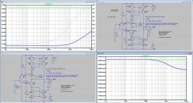
CJE had no effect, but CJC did the job.
ic/vbe is now flat as a ruler for both values of Rload.
Hans
Of course.
Thanks. Here's what I wanted to see. It correlates well with the results of Post 2210. The effect is mostly due to Early. But there's something else there too.
Attachments

With Vaf = 1G and Cjc = 0, both parameters directly concerning the early effect are removed.Hans, which, the Early effect being the explanation? Or the current source-compensated transistor being a problem, or both?
Now with both values for Rload, resp 1 and 1e10, ic/vbe values are equal and flat as a ruler up to 10 Khz.
So the Early effect WAS the explanation after all as it seems.
Not that it worried me a bit, but I enjoyed to sharpening my LTSpice experience and I should have thought myself of changing Vaf, another lesson learned.
But at the end, it doesn't change a bit of how I think of CFA's and VFA's.
Hans
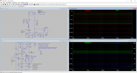
I also sim with increased value of Vaf, crazy values shows ic/vbe almost constant.
With Vaf = 1G and Cjc = 0, both parameters directly concerning the early effect are removed.
Now with both values for Rload, resp 1 and 1e10, ic/vbe values are equal and flat as a ruler up to 10 Khz.
So the Early effect WAS the explanation after all as it seems.
Not that it worried me a bit, but I enjoyed to sharpening my LTSpice experience and I should have thought myself of changing Vaf, another lesson learned.
But at the end, it doesn't change a bit of how I think of CFA's and VFA's.
Cjc (or Cje for that matter) has nothing to do with the Early effect.
There is no Early frequency dependent effect in the Spice modelling of the small signal BJT. For the n-th time, in any AC analysis the schematic is a passive linear RC network with ideal VCCSs. The only frequency dependent model element are the (constant, determined from the bias condition) Cbe si Cbc.
You guys are wasting your time with AC analysis simulations. Transient analysis (nonlinear, including the r0 modulation by vce) can provide some clues, although I have no idea what you intend to prove here.
Last edited:
Hans,
Yes, we have had our Skype skills sharpened, haven't we?
I agree with Scott and you that this doesn't really affect OUR understanding of how CFAs and VFAs work. But perhaps I never made it adequately clear that those who think like the three of us on this topic were NEVER the target of the discussion about this effect.
Question: with Va set to 1G and capacitances removed, is the transistor now a perfect transconductor? Is ic/vbe exactly equal to gm = Ic(DC)/(kT/q)? Or is there some residual error/effect that we have yet to explain? In other words, has this revealed a significant problem with transistor spice models as Ian had maintained, or not?
Last edited:
I don't know whether Cjc is the right cap to change, but my Sims showed clearly that a cap was involved, just as is the extended Pi model.Yes, we have had our Skype skills sharpened, haven't we?
I agree with Scott and you that this doesn't really affect OUR understanding of how CFAs and VFAs work. But perhaps I never made it adequately clear that those who think like the three of us on this topic were NEVER the target of the discussion about this effect.
Question: with Va set to 1G and capacitances removed, is the transistor now a perfect transconductor? Is ic/vbe exactly equal to gm = Ic(DC)/(kT/q)? Or is there some residual error/effect that we have yet to explain? In other words, has this revealed a significant problem with transistor spice models as Ian had maintained, or not?
When not changing Cjc, but placing a -10.4pF cap in par. to the transistor in question has the same effect.
So far for the cap.
But Vaf is definitely the right parameter responsible for Ro.
But there are still many parameters left in the model, so it has not become a perfect transistor IMHO.
Hans
I don't know whether Cjc is the right cap to change, but my Sims showed clearly that a cap was involved, just as is the extended Pi model.
When not changing Cjc, but placing a -10.4pF cap in par. to the transistor in question has the same effect.
So far for the cap.
But Vaf is definitely the right parameter responsible for Ro.
But there are still many parameters left in the model, so it has not become a perfect transistor IMHO.
Hans
Perhaps Ian will weigh in on the extent to which there is or is not a significant problem with LTSpice transistor models. Or maybe someone else.
If you really want to go to the bottom of the sea, yes there is still a small discrepancy between ic/vbe and gm.Yes, we have had our Skype skills sharpened, haven't we?
I agree with Scott and you that this doesn't really affect OUR understanding of how CFAs and VFAs work. But perhaps I never made it adequately clear that those who think like the three of us on this topic were NEVER the target of the discussion about this effect.
Question: with Va set to 1G and capacitances removed, is the transistor now a perfect transconductor? Is ic/vbe exactly equal to gm = Ic(DC)/(kT/q)? Or is there some residual error/effect that we have yet to explain? In other words, has this revealed a significant problem with transistor spice models as Ian had maintained, or not?
We don't know what T LTPice is using, 300K is not uncommon, but 20C or 293K might also be used.
Given the 986.4uA current flowing through our transistor, gm would be 39.1mA/V or 38.2mA/V for resp. 293K and 300K.
What LTSpice calculates for ic/vbe is 37.4 and 37.5mA/V for resp 1 and 1e10 Ohm load, still a few percent differing from gm.
Could this be caused by Rbb?
So I changed Rbb from 170 Ohm in the both models to 1.7 Ohm.
ic/vbe now went to resp 37.8 and 38.0 mA/V for Rload resp. 1 Ohm and 1e10 Ohm.
That's it.
Hans
Last edited:
If you really want to go to the bottom of the sea, yes there is still a small discrepancy between ic/vbe and gm.
We don't know what T LTPice is using, 300K is not uncommon, but 20C or 293K might also be used.
Given the 986.4uA current flowing through our transistor, gm would be 39.1mA/V or 38.2mA/V for resp. 293K and 300K.
What LTSpice calculates for ic/vbe is 37.4 and 37.5mA/V for resp 1 and 1e10 Ohm load, still a few percent differing from gm.
Could this be caused by Rbb?
So I changed Rbb from 170 Ohm in the both models to 1.7 Ohm.
ic/vbe now went to resp 37.8 and 38.0 mA/V for Rload resp. 1 Ohm and 1e10 Ohm.
That's it.
Hans
Sounds great! LTSpice says:
"temp 27°C Default temperature for circuit element instances that don't specify temperature."
Or the temp could be specified:
"This is an archaic form for the step command for temperature. It performs the simulation for each temperature listed.
The syntax
.TEMP <T1> <T2> ...
is equivalent to
.STEP TEMP LIST <T1> <T2> ..."
The syntax
.TEMP <T1> <T2> ...
is equivalent to
.STEP TEMP LIST <T1> <T2> ..."
With temp now known or set, does the Rbb spec still explain all?
If you really want to go to the bottom of the sea, yes there is still a small discrepancy between ic/vbe and gm.
We don't know what T LTPice is using, 300K is not uncommon, but 20C or 293K might also be used.
Given the 986.4uA current flowing through our transistor, gm would be 39.1mA/V or 38.2mA/V for resp. 293K and 300K.
What LTSpice calculates for ic/vbe is 37.4 and 37.5mA/V for resp 1 and 1e10 Ohm load, still a few percent differing from gm.
Could this be caused by Rbb?
So I changed Rbb from 170 Ohm in the both models to 1.7 Ohm.
ic/vbe now went to resp 37.8 and 38.0 mA/V for Rload resp. 1 Ohm and 1e10 Ohm.
That's it.
Hans
But why can't I find a value of negative resistance that keeps ic/vbe constant for ALL values of Rload? There's still a bit of a mystery here.
Early onset (and late offset) effects are understandable from a Thevenin perspective. It is proposed that non-linear Vbe changes are the result of a high impedance load appearing to the inverting terminal as turning into to a low impedance one, being causal of early onset.
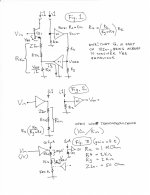
From an earlier post, a Thevenin translation was created whereupon a virtual Thevenin buffer was created to clarify the behaviour of a CFA. Fig. 1 shows a series of 3 resistances that can be calculated in series with the emitter of Q1. I have now added Rx as to complete the resistance path to ground. Rx was translated to be a function of Rz as:
Rx = Rz (Rg/Rg + Rf)
The value of the input stage open loop transconductance is therefore given by:
Vin / (Zin-) + (R Thevenin) + (Rz (Rg/ (Rg + Rf))
This transconductance is mirrored into Rz and results in a Vout equal to closed loop feedback. Figure 3 shows typical calculated values for the open loop transconductance. It can be seen that Rx becomes 500K @gain = 2. This resistance dominates the value of transconductance, diminishing current to 2uAmps.
Under steady state conditions the Thevenin buffer disappears, being undetectable by the In- terminal, hence the value of Vbe diminishes to a value causing 2 uAmp’s to flow through 500K Ohm. Upon input stimulus the Thevenin buffer reasserts itself as revealing a 1.05 K Ohm in the path of Vin. It is this reassertion that is considered causal for the step rise in Vbe identified as early onset.
Attachments
- Home
- Amplifiers
- Solid State
- Current Feedback Amplifiers, not only a semantic problem?