Hi Chris,Hi Ian,
This is to be expected. It is something I have never addressed and certainly never contested.
Please take a look at the tremendous variation in ic /vbe in the attached CFA as we vary the loop gain by changing R_LOAD. (Thanks to Scott Wurcer, whose .asc file of an AD844 I borrowed and modified.)
Certainly the DC operating conditions aren't changing; gm = 1mA q / (k T) for all gains. So why does ic / vbe change so much?
I've done again what I previously did for your 2N3904/2N3906 model.
When in Scott's model changing the 4 input buffer transistors for a Generic NPN / PNP, there is practically no change in Ic/Vbe when changing the load.
However, when placing 230K in parallel to these 4 generic transistors simulating Ro, I get exactly the Ic/Vbe values that you found.
Ergo, again Ro can be fully made responsible for the change in Ic/Vbe.
Hans
Scott,
Further to your Challenge, I have made two different models.
One is based on the Classical long tail topology and the other one on a buffered CFA, thus also being a VFA.
It appears that the classical version is better in all aspects, Noise, Slew Rate and IMD, see table below.
To separate both in the table, one is called VFA and the other one CFA, but they are of course both VFA's.
To prevent too much gain, only R3 is now representing the 20k pot.
Gain can be set from 0 to 10x.
For both cases supply current is just below 10mA.
It is of course possible to change both in a non inverting amps, but input capacitance will then start playing a role when steered from a 20k pot.
Hans
Interesting
Could you please show simulations of both of your "amplifiers" using 20k sin at normal level and when clipping, and a sim of 20k square at half output level.
I'm not interested in the volum control, but how stable your "Amplifers" are.
I see that you have included a C2 "inside" the Pot. Please do the sim without that C.
All the best
Hi Chris,
I've done again what I previously did for your 2N3904/2N3906 model.
When in Scott's model changing the 4 input buffer transistors for a Generic NPN / PNP, there is practically no change in Ic/Vbe when changing the load.
However, when placing 230K in parallel to these 4 generic transistors simulating Ro, I get exactly the Ic/Vbe values that you found.
Ergo, again Ro can be fully made responsible for the change in Ic/Vbe.
Hans
Hans, please advise how you create your generic transistors and maybe post their files if they are not simple to make?
As you have seen, it's an excellent way to find the R and C values of Z(s). In case of the LT1395 resp 125K and 3pF.However, what good is measuring the voltage loop gain without the current loop gain? Some thoughts...
To make this test universal, all that had to be done was to insert 2 x 500K resistors from output to the - Input with a 1F cap to earth in between.
Look at the images, and you will immediate notice that for a VFA, in this case a LT1364 all curves are lying on top of each other, but nevertheless, you have your open loop gain available.The problem here is that the different places of the capacitor in the two circuits violates the Middlebrookian requirement that the return analysis be performed at the same point in the same circuit. I'm skeptical that something like this technique will help us determine the predominant form of feedback.
For a CFA, you will see different output voltages for different values of Rg, but the open-loop gain is always the same.
From this info you can easily calculate Z(s)
And above all, it's a very easy method to separate a CFA from a VFA.
Hans
Attachments
Here You are.Hans, please advise how you create your generic transistors and maybe post their files if they are not simple to make?
You have to measure I(V5)/V(b,e) to get the same data that you found.
Ro in this case is {R} and has to be 230K.
When measuring Ic(Q3)/V(b,e), you will find a constant gm value indepenent of R_Load.
But because Ro is inside the transistor, you need to use I(V5).
Hans
Attachments
Hi Reodor,Interesting
Could you please show simulations of both of your "amplifiers" using 20k sin at normal level and when clipping, and a sim of 20k square at half output level.
I'm not interested in the volum control, but how stable your "Amplifers" are.
I see that you have included a C2 "inside" the Pot. Please do the sim without that C.
All the best
That needs a lot of additional info.
What gain are you looking for to be used with these test ?
And what do you mean with 20K sims, are you interested in THD or what.
And what is your definition of clipping, 1% THD ?
The C however in not inside but outside the pot.
And for the square waves, what slew rate is allowed for the input signal.
Hans
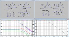
Oops, a small error in the VFA image at the right.As you have seen, it's an excellent way to find the R and C values of Z(s). In case of the LT1395 resp 125K and 3pF.
To make this test universal, all that had to be done was to insert 2 x 500K resistors from output to the - Input with a 1F cap to earth in between.
Look at the images, and you will immediate notice that for a VFA, in this case a LT1364 all curves are lying on top of each other, but nevertheless, you have your open loop gain available.
For a CFA, you will see different output voltages for different values of Rg, but the open-loop gain is always the same.
From this info you can easily calculate Z(s)
And above all, it's a very easy method to separate a CFA from a VFA.
Hans
The three Rg resistors, (Rg, Rg1 and Rg2) should of course all have the same value as in the left image,
But for a VFA this makes no difference at all, so I won't make a new image.
Hans
As you have seen, it's an excellent way to find the R and C values of Z(s). In case of the LT1395 resp 125K and 3pF.
Yes, but you don't even need feedback to do that with a CFA.
To make this test universal, all that had to be done was to insert 2 x 500K resistors from output to the - Input with a 1F cap to earth in between.
Look at the images, and you will immediate notice that for a VFA, in this case a LT1364 all curves are lying on top of each other, but nevertheless, you have your open loop gain available.
For a CFA, you will see different output voltages for different values of Rg, but the open-loop gain is always the same.
From this info you can easily calculate Z(s)
And above all, it's a very easy method to separate a CFA from a VFA.
Hans
Very nice. But please recall that my original question related to applying DIT in an open loop situation, which I thought you stated could be done.
This is useful, though; it could be a great test for determining whether we have a CFA or a VFA. It also puts the lie to the claim that "they're really the same circuit doing same thing."
Here You are.
Hans
May I have the bipolar transistors.lib?
I really do not understand why we need to apply DIT to determine whether a circuit is CFA or VFA.
They are physical configurations that are well defined with specific operating characteristics. We also know that if we raise the loop gain of a CFA, or we apply standard MC, its loop gain morphs into that of a 'classic' VFA. So what - anyone looking for the benefits of a CFA would not do that anyway - in their IC form, and as originally conceived, they were intended for different applications.
They are physical configurations that are well defined with specific operating characteristics. We also know that if we raise the loop gain of a CFA, or we apply standard MC, its loop gain morphs into that of a 'classic' VFA. So what - anyone looking for the benefits of a CFA would not do that anyway - in their IC form, and as originally conceived, they were intended for different applications.
May I have the bipolar transistors.lib?
Attachments
in their IC form, and as originally conceived, they were intended for different applications.
A point often missed, for completeness you tell someone what happens if you use an AD844 at a closed loop gain of 1000, not that there is little point to that.
IC's are general purpose and intended for a broad audience and you need to appeal to all levels of design sophistication and ability.
Hi Reodor,
That needs a lot of additional info.
What gain are you looking for to be used with these test ?
And what do you mean with 20K sims, are you interested in THD or what.
And what is your definition of clipping, 1% THD ?
The C however in not inside but outside the pot.
And for the square waves, what slew rate is allowed for the input signal.
Hans
Sorry I thought it was clear.
Since you are asking:
THD at half output before clipping would be nice. and at 3dB before clipping.
By clipping I mean hard clipping, it should be stable at hard clipping.
About the C you have added:
To have the effect you are using it for the C should be connected from the output to the inverting input of the amp.
What happends if you change the volume by the pot? then it becomes inside the pot if you understand what I'm saying.
By square I mean square.
I really do not understand why we need to apply DIT to determine whether a circuit is CFA or VFA.
ons.
I totally agree
Hi Bonsai,I really do not understand why we need to apply DIT to determine whether a circuit is CFA or VFA..
Well it was Hans Polak Post 1266
But as I showed in Post 1432 it leads to a difficult conclusion. Or would you prefer not to go there because of where it leads? Where dd I read this:As long as Ti is much closer to T, it definitely is a CFA.
If we can agree on that, the discussion has made a Quantum leap forward.
Cheers,"It is error only, and not truth, that shrinks from inquiry." - Thomas Paine
IH
Last edited:
I really do not understand why we need to apply DIT to determine whether a circuit is CFA or VFA. They are physical configurations that are well defined with specific operating characteristics.
DIT would be a fine way to determine the type of feedback predominant in a circuit in which a specific IC is connected to a specific feedback network, but it is not a foolproof means of determining topology.
I think Hans might be moving towards recommending the latest test rather than a DIT to to provide a measurement that confirms topology. That might become useful with some of the newer enhanced designs which might not be so obvious as to type. On the other hand, they might, in which case such a test would not be needed.
We also know that if we raise the loop gain of a CFA, or we apply standard MC, its loop gain morphs into that of a 'classic' VFA.
In what sense? And what does the acronym "MC" stand for?
tired of your slow, limited PC computing power ? use this for free --->
IBM Is Now Letting Anyone Play With Its Quantum Computer | WIRED
-RNM
IBM Is Now Letting Anyone Play With Its Quantum Computer | WIRED
-RNM
Miller compensation.
You can make a VFA with gain-bandwidth independence by returning the Miller compensation capacitor from the VAS collector to the inverting input. Now the unity loop gain frequency is a product/function of the output stage gain (typically unity), Rf and Cmiller. Change the closed loop gain by varying Rg and ensure that the inner (Miller) loop is compensated for the lowest desired gain.
You can make a VFA with gain-bandwidth independence by returning the Miller compensation capacitor from the VAS collector to the inverting input. Now the unity loop gain frequency is a product/function of the output stage gain (typically unity), Rf and Cmiller. Change the closed loop gain by varying Rg and ensure that the inner (Miller) loop is compensated for the lowest desired gain.
- Home
- Amplifiers
- Solid State
- Current Feedback Amplifiers, not only a semantic problem?