Thanks a lot for help! I have another probably very basic question ;-)
I have a sony zx300 portable player, which has a "balanced" headphone out. Balanced in this context apparently only means that the returns/minusses are not shared between the channels (often headphone cables have a common return, so 3 wires in total). So here are 4 wires instead, 2 per channel, and the minus signal of each channel is the opposite of the positive signal, so the voltage amplitude doubles. As I understand it, this is the definition of a differential signal.
In the sony manual they write: "If you use an audio cable to connect the headphone jack (Balanced Standard) to the line-in jack of an audio device, it may damage the device." My understanding is that this would happen if the "audio device" shorts the grounds.
So the question: Can I feed this signal to the JLH, without the sony blowing up?
If not, can it be accomplished with 2 JLH's?
Simulation suggests about 10 Vp or >150 mW, supply voltage limited. That's approaching 120 dB SPL from 97 dB/mW Sennheisers, definitely more than enough. Distortion is above -70 dB at this point, but at deafening volumes like that, who cares.
You could add a single opamp to convert balanced to single ended.
First opamp in figure 22:
Audio Designs With Opamps - 3
First opamp in figure 22:
Audio Designs With Opamps - 3
You could add a single opamp to convert balanced to single ended.
First opamp in figure 22:
Audio Designs With Opamps - 3
Thanks Mooly! Looks simple, am I correct that all that is needed is 4 x 10k plus the opamp? Is this omitting the power supply for the opamp? Which opamp would be recommended for this?
- Could I not also use 2 x JLH's, and only use 1 channel on each (in practice, only fit components for one channel on each, if possible cut away half of the pcb). I don't need the volume control (I think). If so, if sound quality is the only measure, would this be preferred to the opamp?
The opamp could be pretty much any of the well known audio types. The TL071 (TL072 for a dual opamp) would be ideal. Supplies would be anything from -/+ 5v to -/+18
The resistors need to all be equal in value, but absolute value is unimportant. 10k is a good starting point though.
I don't quite follow what you are trying to do with two JLH's. Building just one channel as a separate mono amp still leaves problems if you tried running a pair on the same supply. Even on separate supplies I could imagine all kinds of interaction if you tried feeding the balanced signal to each amp. Doesn't sound a great idea tbh (if thats what you mean).
The opamp could be pretty much any of the well known audio types. The TL071 (TL072 for a dual opamp) would be ideal. Supplies would be anything from -/+ 5v to -/+18
The resistors need to all be equal in value, but absolute value is unimportant. 10k is a good starting point though.
I don't quite follow what you are trying to do with two JLH's. Building just one channel as a separate mono amp still leaves problems if you tried running a pair on the same supply. Even on separate supplies I could imagine all kinds of interaction if you tried feeding the balanced signal to each amp. Doesn't sound a great idea tbh (if thats what you mean).
Thats what my thought was, yes. The difference between a SE and a differential signal seems to me to be that SE is the difference (0 to v+) and the differential is (v- to v+). Problem for me is that SE channels shares the ground so my zx300 would get the v-'s shorted and die. Is this not correct? One mono channel is only 13$ (JLH) and maybe 20$ (transformer), so total costs for 2 sets are still not high. But if you say it would not work well I believe you, I just don't understand why not ;-)
You would have to draw it all out and look at possible conduction paths that could cause trouble but it all just sounds a bad idea tbh. The Sony would drive one JLH OK and would 'float' on the JLH or depending which way you look at it the JLH would float on the Sony output. That would work. When you add a second channel (even a totally separate JLH) there are complex conduction and leakage paths connecting the two such as leakage inductance of the power supplies. It all becomes an unknown but whichever way you look at it its not a great idea.
Use the opamp to convert to SE.
Use the opamp to convert to SE.
You would have to draw it all out and look at possible conduction paths that could cause trouble but it all just sounds a bad idea tbh. The Sony would drive one JLH OK and would 'float' on the JLH or depending which way you look at it the JLH would float on the Sony output. That would work. When you add a second channel (even a totally separate JLH) there are complex conduction and leakage paths connecting the two such as leakage inductance of the power supplies. It all becomes an unknown but whichever way you look at it its not a great idea.
Use the opamp to convert to SE.
Thanks and sorry for thickheadedness
Hi,
Has anyone tried optimising this amp for high impedance cans like HD650 (300ohms)? I would think it's possible to significantly lower the bias current (set by 100R resistor I think) which would lower the operating temperature and reach operating temp sooner, and so make the output DC offset more stable and reach stability sooner?
Has anyone tried optimising this amp for high impedance cans like HD650 (300ohms)? I would think it's possible to significantly lower the bias current (set by 100R resistor I think) which would lower the operating temperature and reach operating temp sooner, and so make the output DC offset more stable and reach stability sooner?
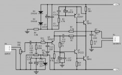
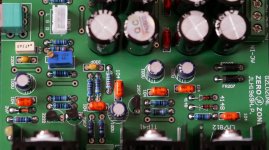
To clarify, I have got the Glozone JLH amp - I've attached the schematic and a photo of one channel.
My suggested changes are:
reduce gain to 4x by replacing R17 470R with 1.5K (done)
C9 appears to be a 100nF not the 33nF in the schematic - try a 10nF poly cap
C13 appears to be 470nF not 1uF - no need to change that I think.
replace ceramic capacitors C11 330p and C15 220p with poly 330p and silver mica 100p
replace DZ1 2.7V zener with two red leds
replace bias resistors R1 5R1 and R25 100R with values up to 50% higher
I haven't checked resistor values or cap polarities yet...
The aim is to improve sound quality of course by customising the circuit for 300ohm Senn HD650 but I also want to make the offset settle faster.
Any tips, comments, etc.? 🙂
Attachments
Last edited:
This looks like an easy work for Prasi....To clarify, I have got the Glozone JLH amp - I've attached the schematic and a photo of one channel.
My suggested changes are:
reduce gain to 4x by replacing R17 470R with 1.5K (done)
C9 appears to be a 100nF not the 33nF in the schematic - try a 10nF poly cap
C13 appears to be 470nF not 1uF - no need to change that I think.
replace ceramic capacitors C11 330p and C15 220p with poly 330p and silver mica 100p
replace DZ1 2.7V zener with two red leds
replace bias resistors R1 5R1 and R25 100R with values up to 50% higher
I haven't checked resistor values or cap polarities yet...
The aim is to improve sound quality of course by customising the circuit for 300ohm Senn HD650 but I also want to make the offset settle faster.
Any tips, comments, etc.? 🙂
I changed the two ceramics for Wima poly caps, and given the lower gain, I chose lower values to push the bandwidth so C11 reduced from 330p to 220p and C15 reduced from 220p to 100p. The treble definition is noticeably better - quite an obvious change and is super clear. Unfortunately, my old scope has died so I can't do any more thorough checks than a DMM and my fairly reliable ears. There is none of the over crispy notes or ringing that would suggest instability. But I miss my scope. Old as it was, it was still really useful to confirm.
C23, C24 : Are shown on both the schematic and the PCB with incorrect polarity
This is still true for the board I just bought and the caps were fitted according to the silkscreen. They had 1.3V DC across them with incorrect polarity. I replaced them with SilmicII inserted in opposite polarity to the silkscreen. I also replaced C1 and C2 with SilmicII following Miles advice that they should be high quality. C1 and C2 are the electros whose negative pin connects to the base of a 2N2907, and positive pin to the collector of a TIP41C.
Component Issues
By design the original JLH version was inherently stable at RF frequency a number of components are not required
- C9, C10 : 33nF However the supplied value is 0.1uf
- C13, C14 : 1uF Are supplied as 0.47uF
- C15, C16 : 330pF Is a ceramic capacitor which will perform poorly in this function
- C1, C2 - C23, C24 : Would benefit from having high quality components
C5, C6 - C19, C21 - C17, C18
The zener diode stated on the schematic diagram 2V7 = 2.7V The supplied value is 3V0 = 3V
Also still true for my new amp.
The zero ohms links supplied are of poor quality and have a value of 0.4 to 1 ohm
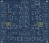
These are now traces instead of wire links, so that seems to have been fixed. There is also a ground pour on the top side to create a ground plane, which the old boards seem to lack.
Thank you Miles ! 🙂
Attachments
Last edited:
Thanks to all who have contributed to this thread - finished reading it at last 🙂
Summary of the changes to pre-built Glozone (one channel is given but of course, both channels were changed):
reduced gain to 4x by replacing R17 470R with 1.5K
replaced ceramic capacitor C11 330p with Wima poly 220p to extend the bandwidth to about 200KHz
replaced ceramic C15 220p with Wima poly 100p for an input low pass below ~300KHz
replaced C23 with 100uF SilmicII with "reversed" polarity to correct silkscreen/schematic error
replaced C1 with 220uF SilmicII
replaced C7 with 100uF SilmicII
replaced R1 5R1 with 10R to lower current through the output transistors to 60mA from 115mA (for a 300ohm load, with a gain of 4x giving max 12V peak to peak output, 40mA is required, so ~60mA is a minimum, subject to critical listening)
I'm leaving those changes to break in before assessing what to do next. Currently, the start up offset is 110mV and falls very quickly to around 70mV. Within 10 mins it is around 20mV. I trimmed it to zero after an hour and it fluctuates within +/-2mV when fully warmed up. A 30VA 12-0-12 transformer gets warm, and the heatsinks are warm but not hot. They were at 55degC with 5.1R and I guess they are a little under 40degC now. This is fine.
Yet to do?
Replace DZ1 and C20 to create a lower noise voltage reference - green led+1n4007 diode? Adjust R21 to fine tune the voltage.
Perhaps reduce R1 to 9.1, 8.2, 7.5, 6.8, etc to see if this improves sound quality
C9 is 100nF not the 33nF in the schematic. This sounds fine and aids stability so perhaps no change needed but try 33nF ... ? I need to look up zobels for HD650 to tailor this to both amp+cans
C13 appears to be 470nF not 1uF - no need to change that given I don't plan to change the input resistance.
The rectifier diodes are fast recovery types with a large cap bank and the 7812/7912 have a large cap bank after them too, so this psu doesn't seem to be limiting the amp. If it ain't broke...?
Attachments

Last edited:
It doesn't sound good :-( Essentially, the tonal balance has changed significantly so it is too warm.
This change is much more than I've ever heard swapping out caps, so I'm certain the change in tonal balance is due to the reduction in bias current by increasing R1 - I would guess that this has significantly increased the output impedance of the amp and that is the cause.
I've read that Sennheiser designed the HD650 300ohm cans to offer optimal damping with low output impedance amplifiers so I would theorise that the amp is now overdamping the cans.
I looked up the specs/measurements. It seems the cable measures at 290pF and drivers are 2.5mH. With roughly 300ohms, 2.5mH and 500pF, that gives a filter node at about 140KHz. Coincidentally, a 22R + 33nF zobel has a similar frequency.
So, next up is to replace C9 (100nF) with the correct value of 33nF, replace the zener reference, and finally vary R1 to get the tonal balance right for HD650.
I betcha it's actually the reduced gain that's giving you trouble (oscillation). You didn't adjust C11-R12. Try removing either - in simulation I found they rather made things worse anyway. I also suggest you try R17 = 1k0 first.
Messing with the gain in amplifiers that aren't explicitly compensated is tricky business. This circuit is most definitely not unity gain stable. I imagine a few pF of Miller capacitance for Q5 (or a few hundred in parallel with R23) may help, but I don't have my JLH sim files here right now.
I would be very surprised if the circuit had more than a few dozen ohms of output impedance open-loop, and it's got like 50 dB of feedback. IOW, R7 should be dominating closed-loop output impedance by far.
As for the zener thingy, I suggest substantially increasing R21. There is no reason for the zener to be running at close to 10 mA. At lower current it'll have higher impedance and its noise will be far more easily filtered. I could see 3k3 working just fine, maybe even 10k.
The ideal replacement for the zener would involve at least 3 Si diodes like 1N4148s (opposite polarity, of course, i.e. just like DZ1 is - incorrectly - drawn now), thermally coupled to Q5-7-9 (but avoiding capacitive coupling of the electrical kind). It now takes a while for your offset to settle because the zener setup has a totally different temperature coefficient than the transistors, and even if it did, it's not running at the same temperature anyway.
I think 3 diodes wouldn't quite cut it in sim though, I needed 4. In practice, I'd be tempted to eliminate the trimpot or rather use it to vary bias current instead, in place of R21 (or in series with it, to avoid accidentally smoking anything). I would measure the required voltage at R19 / pot wiper now and see whether it is within the realm of 3 series diodes to begin with. You can always introduce a bit of extra series resistance if all fails, but it would worsen your thermal drift as it reduces the negative temperature coefficient.
Last edited:
I betcha it's actually the reduced gain that's giving you trouble (oscillation). You didn't adjust C11-R12. Try removing either - in simulation I found they rather made things worse anyway. I also suggest you try R17 = 1k0 first.
My first attempt was to copy the reduced gain others suggested - 2.2K - but this did cause problems with unstable offset, so I tried 1.5K and that was fine. After that, I reduced C11 to 220p and C15 to 100p. I was very pleased with the results of this. The trouble came with reducing the bias current and fitting replacement 100uF caps. I think 1k for R17 is worth a try, thanks. Definitely more gain seems to be a good thing.
Messing with the gain in amplifiers that aren't explicitly compensated is tricky business. This circuit is most definitely not unity gain stable. I imagine a few pF of Miller capacitance for Q5 (or a few hundred in parallel with R23) may help, but I don't have my JLH sim files here right now.
I would be very surprised if the circuit had more than a few dozen ohms of output impedance open-loop, and it's got like 50 dB of feedback. IOW, R7 should be dominating closed-loop output impedance by far.
As for the zener thingy, I suggest substantially increasing R21. There is no reason for the zener to be running at close to 10 mA. At lower current it'll have higher impedance and its noise will be far more easily filtered. I could see 3k3 working just fine, maybe even 10k.
The ideal replacement for the zener would involve at least 3 Si diodes like 1N4148s (opposite polarity, of course, i.e. just like DZ1 is - incorrectly - drawn now), thermally coupled to Q5-7-9 (but avoiding capacitive coupling of the electrical kind). It now takes a while for your offset to settle because the zener setup has a totally different temperature coefficient than the transistors, and even if it did, it's not running at the same temperature anyway.
I think 3 diodes wouldn't quite cut it in sim though, I needed 4. In practice, I'd be tempted to eliminate the trimpot or rather use it to vary bias current instead, in place of R21 (or in series with it, to avoid accidentally smoking anything). I would measure the required voltage at R19 / pot wiper now and see whether it is within the realm of 3 series diodes to begin with. You can always introduce a bit of extra series resistance if all fails, but it would worsen your thermal drift as it reduces the negative temperature coefficient.
It is the thermal characteristics that I'd like to fix more than anything to get faster offset reduction, since noise isn't apparent anyway - a zener+diode would do better for this but I think an LED + diode might be the best compromise. So yes, increasing the resistance to lower the current through the reference makes sense to me, thanks.
The other idea in my head is to modify the output zobel. Correcting HD650 impedance is roughly 360R + 22nF. The amp design is 22R + 33nF. I was considering fitting 22nF and a variable resistor and simply listening to find the best compromise as I adjust the resistance.
Thanks for your help! Much appreciated 🙂
Last edited:
I'm making a servo prototype and right now I do not have the TL1169. Could I replace this with a TL082?
Should do in a pinch. Make sure you've got enough output attenuation to keep its higher voltage noise at bay. You may be left with a few mV of remaining DC offset due to higher Vos spec, but that still is nothing I'd consider in any way critical.
Should do in a pinch. Make sure you've got enough output attenuation to keep its higher voltage noise at bay. You may be left with a few mV of remaining DC offset due to higher Vos spec, but that still is nothing I'd consider in any way critical.
Thanks for the recommendation. It is a simple test, if the prototype works correctly, the version that will go on the amplifier will use the TL1169
- Home
- Amplifiers
- Headphone Systems
- JLH Headphone Amp