You must have the same problem, as everyone else has when using Ians i2stopcm board: The TDA1541a only converts 15 bits.
The distortion, on the other hand, batteryman describes, IMHO, is unique for his setup, as neither you, I or ryanj has experienced that and I haven't seen it described anywhere else using this i2stopcm board with TDA1541A.
See post 6665 - Hanze Khronye describes the same sort of distortion due to the signal "crashing into the DC rail voltage".
It may be different to what I have been hearing, but maybe not, as I tend to listen to small scale classical music where the peaks are fewer and smaller. I don't have any CDs with continuously loud tracks or maybe I'd see the same rail to rail distortion?
I did use WS for LE, but I did not disconnect it from Ian's board.
Unfortunately, I have blown his board by connecting it to 15v during relocation so I have decided to go down EC Design's discrete route instead, with I2S attenuation as well.
Soldering smd parts will be a challenge with my shaking hands and eyesight
(old age) though I may attempt my own version with through hole components, I need inverted data as well. I really could also do with two I2S inputs so I can switch between CD & USB with a 74157 multiplexer.
So story ends here .. I am so sorry to hear your board is dead now. I can tell you ryanj's board is working well and not that difficult to solder.I am a -52 vintage, so my eyes and hands are not what they used to be either. Remember to buy the right parts in the correct housing ( I got some of the IC's in a smaller package first time around)
For others , who wants to correct Ians board: Invert the CLK out of Ians board to TDA1541A, disconnect the LE out from Ians board and connect the LE input on the TDA1541a board to the WS input on Ians board (in parallel with the cable from i2s source to Ians board) . Data input and DL and DR is not changed.
Yes, the story ends and many thanks to all those who contributed.
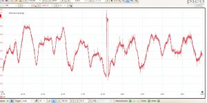
On the subject of the distortion and rail to rail bouncing, consider this:
If you imagine an 8bit dac was fed with a 9bit data. Provided the level stays below 256, all is well. But should the data reach 256, (or above) then the 9th bit will be ignored and the dac will just see eight zeros so the output will switch instantly from 255 to 0. This seems to be shown in the trace below. Obviously you would expect the dac to ignore the LSB not the MSB, unless they were in the wrong order....?
Update. Ryanj still has some pcbs left so I've ordered two. SOIC 1.27mm pitch I can just about manage, but with the desolder braid on hand.
Attachments
Last edited:
You must have the same problem, as everyone else has when using Ians i2stopcm board: The TDA1541a only converts 15 bits.
The distortion, on the other hand, batteryman describes, IMHO, is unique for his setup, as neither you, I or ryanj has experienced that and I haven't seen it described anywhere else using this i2stopcm board with TDA1541A.
Summarizing:
- if I use Ian's I2stopcm board with TDA1541, I will only have 15 bit resolution, since there is a problem creating offset binary mode
- if I use I2Stopcm board to create pcm to AD1865, PCM63, 1702, 1704 and so on, they can be perfect
- to achieve offset binary from I2S the only way now is ryanjs board
- TDA1541 still may be used with I2S, I only have to disconnect the I2Stopcm board and use the I2S signals directly
- missed something?
You are still getting this wrong IMHO.Yes, the story ends and many thanks to all those who contributed.
On the subject of the distortion and rail to rail bouncing, consider this:
If you imagine an 8bit dac was fed with a 9bit data. Provided the level stays below 256, all is well. But should the data reach 256, (or above) then the 9th bit will be ignored and the dac will just see eight zeros so the output will switch instantly from 255 to 0. This seems to be shown in the trace below. Obviously you would expect the dac to ignore the LSB not the MSB, unless they were in the wrong order....?
Update. Ryanj still has some pcbs left so I've ordered two. SOIC 1.27mm pitch I can just about manage, but with the desolder braid on hand.
An 8 bit dac can only be fed by 8 bits . It will ignore the 9th bit.
Lets take 4 bits instead as it involves fewer bits
0000
0001
0010
0011
0101
0110
0111
1000
1001
1010
1011
1100
1101
1110
1111
That is all it understands
If it receives 10111 it will see it as 1011
And it would see 10110 as 1011 as well..
Only loosing the resolution of the 5th bit..
The other thing I believe you are misunderstanding is that the data stream is the same (LSB first MSB last in the serial stream) as in I2S. It can easy be misunderstood if you look at the oscilloscope pictures , as MSB is the leftmost and LSB is the rightmost of the data bits..
The difference is that I2S must have one clk pulse before the data begins. Not so in simultaneous mode. Data is there @ the first clk pulse. No change in the sequence of data ( Same as Left Justified). L and R data must be clocked out simultaneous also in simultaneous mode.
-No has nothing to do with offset binary mode. Ians board is just removing the 16th bit, so TDA1541 is only recieving 15 bits. If TDA1541 think it is 0 or 1 dosent matter, it doesent change! Another problem is that TDA1541A needs an inverted CLK as it clocks data in different from all other DAC'sSummarizing:
- if I use Ian's I2stopcm board with TDA1541, I will only have 15 bit resolution, since there is a problem creating offset binary mode
- if I use I2Stopcm board to create pcm to AD1865, PCM63, 1702, 1704 and so on, they can be perfect
- to achieve offset binary from I2S the only way now is ryanjs board
- TDA1541 still may be used with I2S, I only have to disconnect the I2Stopcm board and use the I2S signals directly
- missed something?
- Yes.
- Still it has nothing to do with offset binary mode or not. Ians board will , as far as I can see, work perfectly, if you invert the CLK from Ians board to TDA1541a board and use WS input to Ians board as input to the TDA1541a as well (parallel connected).
- Of course, but you have to put TDA1541A in I2S mode then. If you use any I2Sto simultaneous mode , you have to change your TDA1541a board to simultaneous mode as well.
Simultaneous mode means, as the word implies, that Left data and Right data is clocked in to the DAC at the same time.
Both boards have the extra feature, that CLK is only present while DAT is there .
You are still getting this wrong IMHO.
An 8 bit dac can only be fed by 8 bits . It will ignore the 9th bit.
Lets take 4 bits instead as it involves fewer bits
0000
0001
0010
0011
0101
0110
0111
1000
1001
1010
1011
1100
1101
1110
1111
That is all it understands
If it receives 10111 it will see it as 1011
And it would see 10110 as 1011 as well..
Only loosing the resolution of the 5th bit..
The other thing I believe you are misunderstanding is that the data stream is the same (LSB first MSB last in the serial stream) as in I2S. It can easy be misunderstood if you look at the oscilloscope pictures , as MSB is the leftmost and LSB is the rightmost of the data bits..
The difference is that I2S must have one clk pulse before the data begins. Not so in simultaneous mode. Data is there @ the first clk pulse. No change in the sequence of data ( Same as Left Justified). L and R data must be clocked out simultaneous also in simultaneous mode.
No I do understand this, I was simply trying to find and explanation for the distortion I and two others have mentioned. I.e what is the cause of the audio break up.
I know the data is left justified and the I am aware of the difference between I2S and simultaneous. So what will be the effect of feeding Ian's board with non I2S data, will this explain the distortion?
No one has stated that this is the reason for the distortion and I'd hate to think I have wasted everyone's time if the cause was that the data was not I2S all along. or is it because of the mistake Ian's made with the 16th bit, & clock polarity?
Last edited:
I fed Ians board with I2S and the output looked precisely as yours, so I don't think so. Both 3lite and ecdesign had predicted that this could not be the case.No I do understand this, I was simply trying to find and explanation for the distortion I and two others have mentioned. I.e what is the cause of the audio break up.
I know the data is left justified and the I am aware of the difference between I2S and simultaneous. So what will be the effect of feeding Ian's board with non I2S data, will this explain the distortion?
No one has stated that this is the reason for the distortion and I'd hate to think I have wasted everyone's time if the cause was that the data was not I2S all along. or is it because of the mistake Ian's made with the 16th bit, & clock polarity?
It could still be because of the non inverted CLK that produces unpredictable results.
You are still getting this wrong IMHO.
An 8 bit dac can only be fed by 8 bits . It will ignore the 9th bit.
Lets take 4 bits instead as it involves fewer bits
0000
0001
0010
0011
0101
0110
0111
1000
1001
1010
1011
1100
1101
1110
1111
That is all it understands
If it receives 10111 it will see it as 1011
And it would see 10110 as 1011 as well..
Only loosing the resolution of the 5th bit..
The other thing I believe you are misunderstanding is that the data stream is the same (LSB first MSB last in the serial stream) as in I2S. It can easy be misunderstood if you look at the oscilloscope pictures , as MSB is the leftmost and LSB is the rightmost of the data bits..
The difference is that I2S must have one clk pulse before the data begins. Not so in simultaneous mode. Data is there @ the first clk pulse. No change in the sequence of data ( Same as Left Justified). L and R data must be clocked out simultaneous also in simultaneous mode.
Not easy... I ****** it up .. MSB first and LSB last 😱
Yes, the story ends and many thanks to all those who contributed.
On the subject of the distortion and rail to rail bouncing, consider this:
If you imagine an 8bit dac was fed with a 9bit data. Provided the level stays below 256, all is well. But should the data reach 256, (or above) then the 9th bit will be ignored and the dac will just see eight zeros so the output will switch instantly from 255 to 0. This seems to be shown in the trace below. Obviously you would expect the dac to ignore the LSB not the MSB, unless they were in the wrong order....?
Update. Ryanj still has some pcbs left so I've ordered two. SOIC 1.27mm pitch I can just about manage, but with the desolder braid on hand.
Please note that the SOT-23-5 and SOT-23-6 packages have a pin pitch of 0.94 mm/37 mil.
Please note that the SOT-23-5 and SOT-23-6 packages have a pin pitch of 0.94 mm/37 mil.
Thanks, I'll be careful!
I have successfully soldered several 64pin TQFP .8mm pitch mcus and I found the best way was to drag the iron and solder over a few pins at a time and then wick up the excess with desolder braid, leaving a clean finish. The pcbs were small so a croc clip worked well for holding it in place.
Ok, this should be child's play for you then. Just wanted to make sure you knew what you were up against. 🙂
Ok, this should be child's play for you then. Just wanted to make sure you knew what you were up against. 🙂
Thanks, I bought two in case I wrecked one. If not, I intend to build a second dac as I have 9 of my dual 1541 pcbs left. The second will use standard dem caps and clocking as a comparision.
I presume I don't need to use any attenuator between your board and the TDAs with it running off 3.6v.
Do you see any advantage in using a 3.2v LiFePO4 cell instead of deriving the supply from the CD player? (A Sony cdp M18 which has a TDA1543 so should provide NOS I2S from the input to the Sony digital filter as with a SAA7220)
Also, I need inverted data so can I just parallel U14 a b with a HC00 ? (although I think this will give a 1LSB error. I thought I might just invert the MSB as this is the sign bit but that doesn't seem to work either)
Last edited:
I presume I don't need to use any attenuator between your board and the TDAs with it running off 3.6v.
You dont need to attenuate, but you could if you want to . You could also use a lower voltage reg like the LP5907MFX-2.5/NOPB instead of the LP5907MFX-3.3/NOPB. I think John suggested this a while back, but im yet to give it a go.
You dont need to attenuate, but you could if you want to . You could also use a lower voltage reg like the LP5907MFX-2.5/NOPB instead of the LP5907MFX-3.3/NOPB. I think John suggested this a while back, but im yet to give it a go.
Do you think using the LP5907MFX-2.5/NOPB is a good idea with your Distinction1 PCB?
I can give that a try and report back.
Inverting the MSB dosen't work as can be seen from this 4 bit example,Thanks, I bought two in case I wrecked one. If not, I intend to build a second dac as I have 9 of my dual 1541 pcbs left. The second will use standard dem caps and clocking as a comparision.
I presume I don't need to use any attenuator between your board and the TDAs with it running off 3.6v.
Do you see any advantage in using a 3.2v LiFePO4 cell instead of deriving the supply from the CD player? (A Sony cdp M18 which has a TDA1543 so should provide NOS I2S from the input to the Sony digital filter as with a SAA7220)
Also, I need inverted data so can I just parallel U14 a b with a HC00 ? (although I think this will give a 1LSB error. I thought I might just invert the MSB as this is the sign bit but that doesn't seem to work either)
1110 = -2 Invert msb 0110 = 6
1111 = -1 0111 = 7
0000 = 0 1000 = -8
0001 = 1 1001 = -7
0010 = 2 1010 = -6
Do you think using the LP5907MFX-2.5/NOPB is a good idea with your Distinction1 PCB?
I can give that a try and report back.
Yeah its worth trying. I'd be tempted to try the 1.8V version too, but it's probably getting a bit to close for comfort.
I ordered the 2.5v and 3.3v as a backup.
Am I correct in assuming that the lower voltage attenuates the signal output in some ways functionally similar to the attenuation circuits on the input of the 1541a pcb?
Am I correct in assuming that the lower voltage attenuates the signal output in some ways functionally similar to the attenuation circuits on the input of the 1541a pcb?
I see in the data sheets that VCC can be 2v to 6v and output voltage and current vary based on VCC. So this suggests the 2.5v is within spec and will result in a lower signal on output. So it sounds like I'll get the attenuated signal as a bonus.
I also note however, that switching characteristics of the SN74HC08 depend on VCC. The transition time and propagation delay are reduced at higher VCC. I wonder if running at lower VCC can introduce timing jitter?
I also note however, that switching characteristics of the SN74HC08 depend on VCC. The transition time and propagation delay are reduced at higher VCC. I wonder if running at lower VCC can introduce timing jitter?
Similar effect. Less swing, less RF energy entering dac.I ordered the 2.5v and 3.3v as a backup.
Am I correct in assuming that the lower voltage attenuates the signal output in some ways functionally similar to the attenuation circuits on the input of the 1541a pcb?
- Home
- Source & Line
- Digital Line Level
- Building the ultimate NOS DAC using TDA1541A