Hi, this is my newest design, mosfet CFA, unusually compensated - output inclusive alexander compensation. The result is superb, very low thd, high SR, good PSRR. I would like to know your opinion, what to improve and so. thx
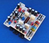
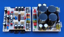
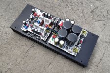
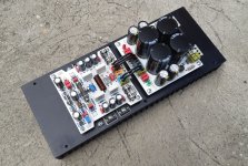
The PCB is nearly finished, dimension 10x10cm, the PSU is on separate board, also 10x10cm.


View attachment K61-VMOS-OIAC.asc
The PCB is nearly finished, dimension 10x10cm, the PSU is on separate board, also 10x10cm.
View attachment K61-VMOS-OIAC.asc
Hi LKA
That looks very good!
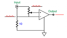
A suggestion. An input ground break 10 ohms is helpful.
BTW John Broskie discusses it here Line Stages and Kicking Butt His relevant circuit is attached. A "House-Gnd" breaker is also helpful. It's mentioned further down in the article.
Are R14,R16 supposed to be a trimpot for offset trim?
What does the clip overload recovery look like? Eg 20kHz sine input.
That looks very good!
A suggestion. An input ground break 10 ohms is helpful.
BTW John Broskie discusses it here Line Stages and Kicking Butt His relevant circuit is attached. A "House-Gnd" breaker is also helpful. It's mentioned further down in the article.
Are R14,R16 supposed to be a trimpot for offset trim?
What does the clip overload recovery look like? Eg 20kHz sine input.
Attachments
Excuse my ignorance but how the LEDs D5, D6 will contribute to the whole schematic's performance? And the same question for C1, C5?
Beside that I suppose that schematic's PSRR will be pathetic. I'm stressing on this because according to my small experience this is one of the most important factors defining the good or bad sound of the CFAs.
The output stage is not significant since anyone can design something similar with BJTs, LAT-MOS, VD-MOS etc...
Hi LKA
That looks very good!
A suggestion. An input ground break 10 ohms is helpful.
BTW John Broskie discusses it here Line Stages and Kicking Butt His relevant circuit is attached. A "House-Gnd" breaker is also helpful. It's mentioned further down in the article.
Are R14,R16 supposed to be a trimpot for offset trim?
What does the clip overload recovery look like? Eg 20kHz sine input.
All my amps use dual-mono concept. In that case it is better to ignore the 10R resistor and connect the cold terminal of the input RCA to the chassis with parallel combination of resistor and cap.
yes, R14,16 - trimpot for offset trim
Well, 20k clipping is not the best, I can improve it but I'm not sure it worth the effort. (1k clipping is clear)

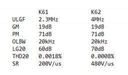
PSRR is not excellent but quite good. If you look at my previous design K51 - 120W/4R CFA POWER AMPLIFIER - Google Photos which uses the same front-end except the cascode in second stage (summing node), you find measurements. The cascode improves the PSRR about 12dB, so, the result will be even better.


Excuse my ignorance but how the LEDs D5, D6 will contribute to the whole schematic's performance? And the same question for C1, C5?
Beside that I suppose that schematic's PSRR will be pathetic. I'm stressing on this because according to my small experience this is one of the most important factors defining the good or bad sound of the CFAs.
The output stage is not significant since anyone can design something similar with BJTs, LAT-MOS, VD-MOS etc...
D5,D6 - VAS current limiters
C1 and C5 increase VAS amplification starting at about 1kHz. 100R degeneration resistor alone does not allow loop gain that can be shaped what you see in the first post.
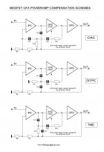
attached pictures
1. no compensatiom at all
2. C1,C5 in place, no other comp


I simulated it and my distortion result differs from yours. I used your Ltspice file and just changed 10V zeners as I don't have those you used.
THD results at 100W/4ohm
THD1k=0.0047%
THD20k=0.0021%
Strange thing is so high distortion at 1kHz.
I simulated this amp with better IRF mosfets models, and here is result:
THD1k=0.0036%
THD20k=0.0026%
I noticed some error in your file, in the Thian probe the current source is up side down.
Some comments:
In my opinion diodes D5 and D6 not needed, and they increase distortion.
I am not sure D3 and D4 will protect output mosfet in case of high transient impuls at the input. As those diodes are revers polarized in normal operation the diode capacitance ih highly non linear, so higher distortion.
Damir
Attachments
I simulated it and my distortion result differs from yours. I used your Ltspice file and just changed 10V zeners as I don't have those you used.
THD results at 100W/4ohm
THD1k=0.0047%
THD20k=0.0021%
Strange thing is so high distortion at 1kHz.
I simulated this amp with better IRF mosfets models, and here is result:
THD1k=0.0036%
THD20k=0.0026%
I noticed some error in your file, in the Thian probe the current source is up side down.
Some comments:
In my opinion diodes D5 and D6 not needed, and they increase distortion.
I am not sure D3 and D4 will protect output mosfet in case of high transient impuls at the input. As those diodes are revers polarized in normal operation the diode capacitance ih highly non linear, so higher distortion.
Damir
You're right, thd1k is strange. Some days ago I've changed driver transistor to MJE, I used 2SC4793/2SA1837 before. Let's try this file - K61.asc
D5,D6 - When output is shorted, D3,D4 become forward biased and draw excess current from VAS.
View attachment K61.asc
You're right, thd1k is strange. Some days ago I've changed driver transistor to MJE, I used 2SC4793/2SA1837 before. Let's try this file - K61.asc
D5,D6 - When output is shorted, D3,D4 become forward biased and draw excess current from VAS.
View attachment 700617
In my CFA I used 2sc3503/2sa1381 as a drivers. Could be that MJE 15034/35 have to high Cob, datasheet does not show it.
the prototype was born, works as expected (very close to simulation)
Rated Power: 150-200W/4R
Input Impedance: 10kOhm
Sensitivity: 1Vp/100W/4R
Noise: -94dBV,ref 1Vrms,bw20kHz (input shorted)
Slew Rate: 200V/us
THD sin1kHz: <0.001% 1-100W/4R5
THD sin20kHz: <0.002% 1-100W/4R5 (measured before output coil)
Rated Power: 150-200W/4R
Input Impedance: 10kOhm
Sensitivity: 1Vp/100W/4R
Noise: -94dBV,ref 1Vrms,bw20kHz (input shorted)
Slew Rate: 200V/us
THD sin1kHz: <0.001% 1-100W/4R5
THD sin20kHz: <0.002% 1-100W/4R5 (measured before output coil)
Attachments


very nice!
appreciate the update on actual build!
mlloyd1
THX 😀 performance is even better than looking
the photo album K61 - CFA MOSFET POWER AMPLIFIER - Google Photos
Last edited:
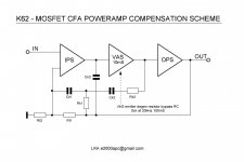
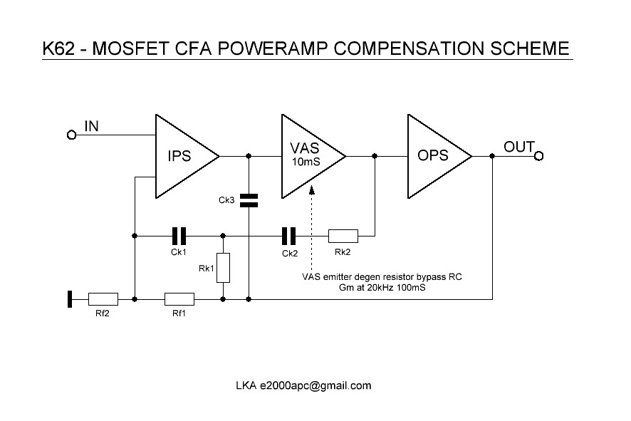
Meanwhile I improved the compensation scheme by adding caps (Ck3x) from output to the VAS input.
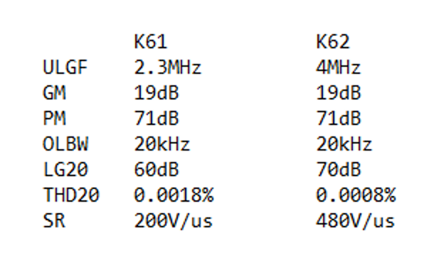
Nice, now you do similar to my OITPC. Your is TMC + Cherry cap.
BR Damir
have you tried in real amp?
have you tried in real amp?
not yet but soon
TMC ? not exactly, then Ck1 would go to the VAS input. Btw, it's not good idea, limits slew rate.
Ck3 - better PM and GM
Attachments
Last edited:
In my simulations, using your models, these are the the best bet.In my CFA I used 2sc3503/2sa1381 as a drivers. Could be that MJE 15034/35 have to high Cob, datasheet does not show it.

- Home
- Amplifiers
- Solid State
- Vmos Super CFA OIAC