It is nice to see you pushing on with this even if I don't completely understand the purpose just now. Probably I am missing something, but aren't all three of the results above as expected?
I've not seen your particular arrangement for adjusting K2 level before but isn't it effectively just an attenuator for the input to the PMOS FET, thereby better matching the contribution of the NMOS FET?
My purpose was to confirm that gm matching between the NMOS and PMOS FETs has its primary affect on the even harmonics and little affect on the odd harmonics.
"... isn't it effectively just an attenuator for the input to the PMOS FET, ..." That is exactly what it is.
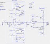
The simulations in post #1579 were with a "perfect" front-end having a 200R output impedance, and no feedback from the OS. I added the gm adjustment circuit to my full ZD25 simulation but have not yet found satisfactory parameters. I tried to get a close approximation to the perfect FE and no global feedback by applying all of the feedback from the FE output. So far the result has been much poorer falloff of the harmonics as the frequency increases. Perhaps the Rxgm1 and Rxgm2 resistors are feeding OS output signal back to the FEOut node in a positive feedback manner which is disrupting the FE feedback loop. I need to try adding a buffer between the FE output and the OS bias drive network to verify that speculation.
Attachments
The undesirable behavior of the Xgm adjustment circuit in my full simulation was due to an unrelated, recently introduced circuit bug in my bias circuit. Having isolated that problem, I will proceed with further tests of the gm adjustment trick.
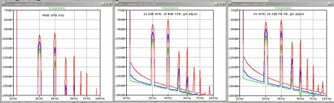
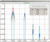
Here are some nice results comparing 3 different feedback arrangements combined with the gm adjustment "trick". From left to right:
- Global feedback only, no OS gm adjustment.
- 13.3dB global feedback, 10.9dB cascode feedback, and OS gm adjustment.
- No global feedback, 24.2dB feedback from FEOut, and and OS gm adjustment.
Attachments

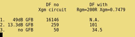
There is a significant difference in damping factors for the three feedback schemes shown in the previous post. Obviously, more global feedback increases the damping factor, as shown below. The gm adjustment "trick" significantly reduces damping factor.
Attachments
Last edited:
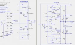
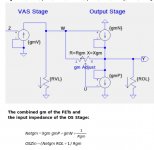
I have done more analysis of the OS stage gm adjustment circuit in post #1579. In the schematic below the resistors Rxgm1 and Rxgm2 are replaced by a pot. The DC circuit equations give the combined gm of the two FETs and the input impedance of the OS stage with the gm adjustment pot. When there is no gm adjustment pot, Rgm is infinite and the OS state DC input impedance is infinite. The VAS stage is loaded by the parallel combination of the VAS load resistor RVL and the OS state input impedance. When the VAS load is very high then the combined load on the VAS stage is significantly changed by Rgm.
Example: gmN=2.86S, gmP=3.57S, ROL=8R. Rgm=200R
Netgm= 5.5425S OSZin=9068R
When RVL=16K (bias spreader load), total VAS load is 5788R
When RVL=1K, total VAS load is 900R.
Bottom line: The gm adjustment circuit load on the VAS stage is not horrible when RVL is significantly small, such as 1k. Increasing Rgm will increase the capacitive effects due to the PFET gate capacitances, increasing distortion at high frequencies.
Attachments
Another possible use of the gm adjustment pot is to balance the DC K2, which is determined by the FET transconductances, against the AC K2, which is determined (primarily) by the FET capacitances. In this way is might be possible for K2 to be largely independent of frequency without massive amounts of negative feedback.
Here are some nice results comparing 3 different feedback arrangements combined with the gm adjustment "trick". From left to right:
The spectral plots are for 1kHz, 1W, 5W, and 25W into 8R load. The outputs for the different power levels have been normalized so that the fundamental is at 0dB.
- Global feedback only, no OS gm adjustment.
- 13.3dB global feedback, 10.9dB cascode feedback, and OS gm adjustment.
- No global feedback, 24.2dB feedback from FEOut, and and OS gm adjustment.
option 3 has one cascode feedback left in the schematic.
Martin
The remaining cascode FB resistor was to minimize K2 of the FE without the load from the OS. The same result could have been obtained by carefully balancing the JFET transconductances without any need for cascode FB resistors. The F5 V2 with the P3 pot allowed the adjustment of K2 by changing the JFET source resistors, which changed the balance of the open-loop gain between the upper and lower halves of the amplifier.
The remaining cascode FB resistor was to minimize K2 of the FE without the load from the OS. The same result could have been obtained by carefully balancing the JFET transconductances without any need for cascode FB resistors. The F5 V2 with the P3 pot allowed the adjustment of K2 by changing the JFET source resistors, which changed the balance of the open-loop gain between the upper and lower halves of the amplifier.
Thank you for the explanation!

Is that a Kairos speaker in your avatar?Thank you for the explanation!
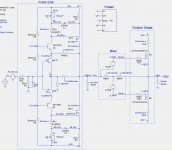
Here are some interesting plots and their circuits. In all cases, there is no global feedback, instead FEOut is connected to the feedback network. The 1k FE load resistor results in 24dB feedback from FEOut and 44dB open-loop gain (with the 1k FE load).
- The top rows are for the complete ZD25 amplifier.
- The bottom rows are for a "perfect" FE.
- The left columns are with the gm adjustment of 200R and X=0.7497
- The right columns are without the gm adjustment pot.
Attachments

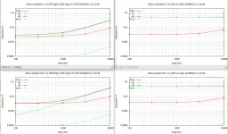
Impressive. So the main drawback without any global feedback is the reduced damping factor (~34R here?)? Out of interest, how does the behaviour change into lower loads, e.g. 4R?
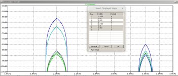
Here is a comparison of the spectra at 1kHz, 5W with 4R and 8R loads. The trace colors are:
Id = Kp/2*(Vgs-Vth-Id*Rs)^2 * (1+lambda*Vds)
- Green
- Blue
- Red
- Cyan
Id = Kp/2*(Vgs-Vth-Id*Rs)^2 * (1+lambda*Vds)
Attachments
Thank you!
So there appears to be no single value of Xgm that optimises K2 for all loads. Unfortunate but then not exactly unexpected either. I notice that the Xgm values for best performance into 4R and 8R are quite close - does this indicate that the adjustment is quite sensitive in general?
I'm seeing similar behaviour whilst exploring more bias issues but I put this down to the gm difference between the output FETs causing increasing mismatch with increasing current. Perhaps this has to do with the non-linearities you mention?
Some additional perspective: Here are some spectral plots that show K2 and K3 with "optimal" values for Xgm (light and dark green between -86dB and -89dB), a value for Xgm that equalizes K2 (gray trace at -86dB), and Xgm=1 (no gm adjustment, the blue and cyan traces at -56dB and -64dB). You can see that K2 at the suboptimal value Xgm=.76 isn't really that different from the optimal values.
Attachments
Do you see any increase in noise at the output as a result of adding your gm adjustment? I find that adding even a small resistance, e.g. 10R in series with the input increases noise from just less than 1uv to 10uv.
- Home
- Amplifiers
- Pass Labs
- F4 Beast Builders