Mark4. I have another board as you. Every delta sigma dac has pre and postringing. With filter settings are changeing. Please post your measurement of 1khz square wave out of the dac... Not opamp stage. I wrote that opamp stage don*t interest me. I don*t need to move jumpers so settings can*t be wrong.
Impuls60. Was any pairing with apple remote necessary?
Thank you.
Impuls60. Was any pairing with apple remote necessary?
Thank you.
Last edited:
Mark4. I have another board as you.
The minimum phase filters do have post-ringing. They do not have pre-ringing. Do we agree on that? If not, we probably need to figure out why.
By the way, when CDs at 16/44 are upsampled to 24/192, just about all the filter junk is up above the audio band where is it inaudible, and as a side-benefit harmonic distortion happens to be reduced (which we saw in measurements). In addition, it sounds *really* good. Of course, SRC4392 is rated for less than -140dB distortion. So even if you get the ES9038Q2M distortion down to -120dB, the best it can be, the SRC4392 doesn't cause sound quality problems. It sounds much, much better than without the SRC. Doesn't matter if other SRC in the past didn't work out well, this one does (at least it does if the other mods are done, haven't tried it without them).
Last edited:

Impuls60 can you post a link of a remote seller. My don*t response to dac.
Mark. In terms of qiuck pulse shot you have right about ringing. I mean at square response that is huge ringing. You know what i mean. You have documentation for es9038q2m maybe you can reveall why your board has 1.2V regulator new board not. Or it has internaly regulator that is hardware or software enabled. At my dac pin 15 has a classical smps noise pattern which trought capacitors polute gnd and trought caps again polute nearby supply pins. One good thing is that es9038q2m has muuuuch smaller noise on output.. I think similar as Ak449x so not much noise get in first opamp even in current mode. Thank you
Mark. In terms of qiuck pulse shot you have right about ringing. I mean at square response that is huge ringing. You know what i mean. You have documentation for es9038q2m maybe you can reveall why your board has 1.2V regulator new board not. Or it has internaly regulator that is hardware or software enabled. At my dac pin 15 has a classical smps noise pattern which trought capacitors polute gnd and trought caps again polute nearby supply pins. One good thing is that es9038q2m has muuuuch smaller noise on output.. I think similar as Ak449x so not much noise get in first opamp even in current mode. Thank you
why your board has ...
I don't know why, there should always be an internal one that just needs decoupling at the pin. Maybe external makes less noise? I don't know. If the DAC board was better designed there would be separate digital and analog ground planes so noise would be less of an issue. I guess one doesn't get that for $39, or whatever the boards go for these days.
Regarding ringing, I don't think it should be an issue if using upsampling. In theory reconstruction filters should not be audible, but in reality the ones that come built into DACs are. That is a problem, as they should not be audible. The best solution I know of is to upsample, and if using a PRO chip then also perform reconstruction filtering in external DSP and make a better filter there (can't do external reconstruction filtering with Q2M though, although [1] custom internal reconstruction filter coefficients could be done in Q2M and might possibly make some sense to implement if upsampling before the DAC with an external SRC board as I recommend {just haven't looked into the details}, and although [2] the other internal Q2M filter, the 'upsampling' filter, could be done externally but it would take a lot of DSP horsepower to do at high sample rates). Also, if using external upsampling then may as well use minimum phase slow transition reconstruction filter since the transition band would be well above any audio frequencies, and since that particular filter has the least group delay of any of the filters and group delay could still be audible (I think).
Last edited:
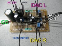
Here it is and I forgot to connect the op amp power underside but basically done
Next stop is to start hacking up the DAC board
Just wonder why do you need extra +12V? What op amps will be used on that board?
And with a single dual opamp for the output stage I would leave it in the original socket, reworking surrounding parts. AVCC buffer goes underneath. Less wires and no drilling IMHO.
Last edited:
This is the remote that works with 1.07 board, Fasdga MC377LL/A Remote Control fit for Apple TV 2 3 Gen Mac Music System I5E3 192090219575 | eBay
On the pictures I posted earlier you can clearly see that the direct line between pin15 gnd and main gnd pin goes very near the the chip and crosses the output signal( in the ground layer). I would assume putting noisy gnd current here would affect the traces above? Would it be better to put pin 15 gnd pin into a wire and route it separately to main gnd pin?
On the pictures I posted earlier you can clearly see that the direct line between pin15 gnd and main gnd pin goes very near the the chip and crosses the output signal( in the ground layer). I would assume putting noisy gnd current here would affect the traces above? Would it be better to put pin 15 gnd pin into a wire and route it separately to main gnd pin?
Last edited:
I am struggling with through hole as it is , Surface mount is a no go for me. No skills there and not possible when I am this old. The other thing is that most of the parts were in my old parts box. There are some parts in there that date back to the early 1980s no late 70s actually 1979 to be exact.Just wonder why do you need extra +12V? What op amps will be used on that board?
And with a single dual opamp for the output stage I would leave it in the original socket, reworking surrounding parts. AVCC buffer goes underneath. Less wires and no drilling IMHO.
I will be running the complete DAC including the IV from a SINGLE 12V. no Negative 12V. This aspect would also require more work on the DAC board. The other aspect is that the DAC remains fully digital and the grounding area is all fully digital as well. Off board will all be analog. Hopefully that helps with noise. Also the reason why I stepped back to this board rather than stage 2 is to discover just how good this DAC can be without special parts. The parts used were primarily in my parts bin.
The other reason is that in the next iteration...
Stage 1.5 - I will compare whether the LT3042 makes any difference to powering the digital. Maybe it will help the clock with a more stable voltage. This is easily done by bypassing the 3 term reg and AMS1117 on board and connecting 3.3V directly to the solder tab/heatsink on the ams117.
stage 2. Which will occur when all this simple circuit sampling is done, it will have a similar circuit but will sport multiple transformers, low Z, low noise power supplies, separate low noise reference for AVCC source voltage via LT3042, triple op amp IV stage per ESS
Stage 3. Upgraded crystal. 3.5 maybe upsampler.
Stage 4. I will add a switchable selector to use a Borbeley hybrid tube based balanced to single ended converter. That way I can use the DAC all day in solid state but when I want to tube effect, I can then power up that stage with a switch that turns on the stage, allow it to stabilize and then switch from op amp to tube. That way I don'r wear out the tubes by having it on for casual listening.
So here is a potential map for the DIYer and the stages one can take this. What the results will be? We'll see.
Last edited:
If successful, I will show the underside of the layout as it will help others. Let's see if it works first. The cost of the board is maybe $5-10 in parts and should be doable by most DIYers.
Well, I think I may have misspoken a few posts ago about internal and external filtering. After having taken a slightly deeper look than previously it looks like oversampling filter, FIR filter, and reconstruction filter might just be different ways of referring to the same thing or different parts of the same thing. Still don't know but would have to ask for clarification myself before forming a firm opinion on what is and isn't possible for Q2M in terms of offloading some processing. Still don't think it would make much sense to add external DSP to this project so I will leave that hypothetical issue off here.
I can verify that using a lifepo4 while simultaneously charging it with a linear supply sounds indistinguishable from using the battery alone vs just the linear supply (two LM317s in series). This has been known to a few people for a while now but just confirming again.
I replaced the usb-powered analog section of the Hifime (dual opa2134s feeding an OPA1622) with a TPS7XXX +-12v I had sitting around. Very nice. Tempted to replace the main 80hz clock but the can type is a PITA, especially with lead-free solder.
I replaced the usb-powered analog section of the Hifime (dual opa2134s feeding an OPA1622) with a TPS7XXX +-12v I had sitting around. Very nice. Tempted to replace the main 80hz clock but the can type is a PITA, especially with lead-free solder.
Many people do repairs with leaded solder around here. Sometimes 63/37 alloy to keep temps low as possible and help overheating adjacent areas.
Many people do repairs with leaded solder around here. Sometimes 63/37 alloy to keep temps low as possible and help overheating adjacent areas.
I meant the solder used by Hifime is likely lead-free, which I find harder to desolder, especially with a multilayer board.
Ah, yes. Using Chip Quik alloy can help greatly. What I have done sometimes is to destroy into pieces a device soldered to the board so I can heat and pull out one pin at a time. Once pins are out either add a blob of soft leaded solder or chip quik alloy to mix in with the remaining unleaded solder in the holes, then either heat and slam down on the bench to expel hot solder or heat and push a hot stainless steel sewing needle through the hole. Since the needle is stainless, solder won't stick to it. Twist and pull to work it out of the hole after the solder has cooled enough. (Chip Quik works so well it is almost like cheating.)
Also, what I like to do is test the solder on the board first by setting my iron temp low then gradually trying higher temperatures until the solder just starts to soften, keep going until it melts fully. That gives me a good idea of the minimum heat I will need to melt the solder initially and get it to mix with removal alloy or softer leaded solder. Adding plenty of extra flux can help prevent oxidation of solder which once that happens makes it harder to remove. Only thing then is to keep adding fresh solder and flux to mix it with it.
And of course, practice on scrap boards first. 🙂
Last edited:
Ah, yes. Using Chip Quik alloy can help greatly. What I have done sometimes is to destroy into pieces a device soldered to the board so I can heat and pull out one pin at a time.
Yeah, that seems the likely path. Hate to have to destroy the clock to replace.
In other news, I see my AVCC pins are bypassed by just 10uf OSCONS (I thought they were discontinued) and a ceramic cap, so should I be increasing that value? Earlier comments seem to indicate AVCC cap values should be much higher.
Attachments
Where is the AVCC power coming from? Just to get an idea of what someone did awhile ago to make a good DAC out of an ESS chip, it seems to me there was a service manual for an old obsolete version m-dac kicking around out there somewhere. IIRC, in the last few pages there is a partial schematic that shows the power supplies including for AVCC, which happen to be all analog. Interesting how much effort they went to in order to get clean enough power. Also, easy to see why it may have been worth some other effort for Benchmark to figure out how to make some type of switcher work for their DACs.
Where is the AVCC power coming from? Just to get an idea of what someone did awhile ago to make a good DAC out of an ESS chip, it seems to me there was a service manual for an old obsolete version m-dac kicking around out there somewhere. IIRC, in the last few pages there is a partial schematic that shows the power supplies including for AVCC, which happen to be all analog. Interesting how much effort they went to in order to get clean enough power. Also, easy to see why it may have been worth some other effort for Benchmark to figure out how to make some type of switcher work for their DACs.
AVCC is coming from the lifepo4 (the picture above was pre-mods)
Okay. How far away are the batteries and what kind of wire? Are we trying to compensate for resistance, inductance? ESS seemed to think having the power source very close to the AVCC pins was important. But they only used electrolytic caps at the output of the AVCC opamps.
- Home
- Source & Line
- Digital Line Level
- ES9038Q2M Board