Good evening guys, and thank you for this wonderful topic about this board;
I have try to read all of the pages but I have one doubt
I' have a pi3 b+ ;
Can I attach one of this boards to my Rpi directly via i2s?

or

and play dsd files?
I see 5 pins for i2s, but raspberry only have 4?
Is missing MCLK on rpi?
Thank you if someone can help..
I have try to read all of the pages but I have one doubt
I' have a pi3 b+ ;
Can I attach one of this boards to my Rpi directly via i2s?
or
and play dsd files?
I see 5 pins for i2s, but raspberry only have 4?
Is missing MCLK on rpi?
Thank you if someone can help..
So I opted to use something more stable or the likelihood of stability is greater.
Not sure how you are planning to do that with two opamps. Parallel opamps require series resistors or some way to allow them to have different input offset voltages. If series resistors then the low output impedance for AVCC will be made worse. Maybe you could only use a series resistor for one but then you might be getting back into questions about stability. Its concerns like that made me ask you to post some kind of a proposed schematic. If we could see what you have in mind then it might raise some questions for discussion.
Last edited:
Markw4, those oscillations are the very reason why when my parts bin is done I am done. There is no way some guy like me with no instrumentation can put something decent without a guess.
Anything is probably better than nothing. It's not much but, there is always something like this: Hantek 6022BE Pc-based USB Digital Storag Oscilloscope 48msa/s 20mhz 2 Channels | eBay
20MHz is enough for many practical purposes, although more MHz is better.
EDIT: Lower price: Hantek 6022BE 20MHz 48MSa/s Handheld 2 CH PC USB Digital Storage Oscilloscope | eBay
Last edited:
What I have not figured out as yet is that my offset divider is on the external board. Do I need to bring that back to the 3038q2m board?
The offset divider, or 'reference voltage,' is 1/2 of AVCC and is only used by the I/V converters, whichever board you have them on.
Remember, you can use adhesive backed copper foil to make a rather thin but better than nothing ground plane. Good for returning bypass caps and such. Keeps return inductance low.
For DSD, use the DATA pin for DSD Data2 (R), use LRCLK pin for DSD Data1 (L), and use BCLK pin for DSD Bit Clock. Not that I have tried it, but I think that is how it works or should work. You may also need to set jumpers to put the DAC in DSD mode. Depends on the particular board. If they say it supports DSD it should work one way or another.
Last edited:
Good evening guys, and thank you for this wonderful topic about this board;
I have try to read all of the pages but I have one doubt
I' have a pi3 b+ ;
Can I attach one of this boards to my Rpi directly via i2s?
or
and play dsd files?
I see 5 pins for i2s, but raspberry only have 4?
Is missing MCLK on rpi?
Thank you if someone can help..
Hi,
Using i2s, I think you can only play dsd files using Dop but not direct DSD.
Hi,
Using i2s, I think you can only play dsd files using Dop but not direct DSD.
Q2M supports 32-bit 768kHz PCM, DSD256 via DoP, and native DSD512 (or possibly native DSD1024, I am a bit sketchy on some of the DSD modes) in master or slave timing modes. Assuming a 100MHz clock is used, that is. And in this case, if the Chinese DAC microcontroller is programmed to support the mode. Don't think it supports master timing at all based on the overall board design.
Last edited:
Thank you very much!!
I don't care if native or dop..
I'm using volumio on raspberry now, with a jlsounds ak4490 with usb.
Who knows if this board will be sound better??
Thank you again!!
I don't care if native or dop..
I'm using volumio on raspberry now, with a jlsounds ak4490 with usb.
Who knows if this board will be sound better??
Thank you again!!
Last edited:
on the first board u have to solder a "socket" or similar to it..Good evening guys, and thank you for this wonderful topic about this board;
I have try to read all of the pages but I have one doubt
I' have a pi3 b+ ;
...
and play dsd files?
I see 5 pins for i2s, but raspberry only have 4?
Is missing MCLK on rpi?
you need only 4 "lines"->Data,LRCK,BCK,GND..
An externally hosted image should be here but it was not working when we last tested it.
MCLK is "provided" by the board/is on the board..
playing native DSD is still tricky/i myself had a few times DoP (Moode,Volumio,Foobar2000+DSD-processor) but still no "native DSD" to be honest and if i hardly remember..some say it is possible and they got it to work, but here to be honest i had no "native DSD" till now..
and very interesting is what "Markw4" has posted:
Q2M supports 32-bit 768kHz PCM, DSD256 via DoP, and native DSD512 (or possibly native DSD1024, I am a bit sketchy on some of the DSD modes) in master or slave timing modes. Assuming a 100MHz clock is used, that is. And in this case, if the Chinese DAC microcontroller is programmed to support the mode. Don't think it supports master timing at all based on the overall board design.
good luck !! 🙂
Last edited:
Not sure how you are planning to do that with two opamps. Parallel opamps require series resistors or some way to allow them to have different input offset voltages. If series resistors then the low output impedance for AVCC will be made worse. Maybe you could only use a series resistor for one but then you might be getting back into questions about stability. Its concerns like that made me ask you to post some kind of a proposed schematic. If we could see what you have in mind then it might raise some questions for discussion.
Markw4. I came to same conclusion afterwards. I thought about balancing currents and then feedback and resistors etc. Then decided looked again at the currents and I think that as long as I use one op amp per channel, then I am covered unless maybe DSD comes into play. I currently only use PCM and it is sounding better than ever with this DAC so far. So I am sticking with PCM for the time being. If this turns out right and I never thought this board could sound so good. Even MP3s are not so bad after all with this DAC at this point.
You literally hear things now that stick out that you missed before.
So the circuit I am building are the identical circuits from ESS "maximizing DAC performance for every budget". Except that the AVC conditioner op amp will be +-15V because the second op amp on the same body will house the Balanced to Single Ended output.
So two dual op amps will provide AVCC conditioner and the three op amp IV circuit and single ended output.
Last edited:
If using the LT3042/5, I *highly* recommend using two in series for lower noise if not done already.
on the first board u have to solder a "socket" or similar to it..
you need only 4 "lines"->Data,LRCK,BCK,GND..
MCLK is "provided" by the board/is on the board..
playing native DSD is still tricky/i myself had a few times DoP (Moode,Volumio,Foobar2000+DSD-processor) but still no "native DSD" to be honest and if i hardly remember..some say it is possible and they got it to work, but here to be honest i had no "native DSD" till now..
and very interesting is what "Markw4" has posted:
good luck !! 🙂
Thank you sfb2!!
I really appreciated
If using the LT3042/5, I *highly* recommend using two in series for lower noise if not done already.
Yes, at the least.
LT says they are "for powering noise sensitive RF applications." They don't say for audio applications. When they say 'mixers' they mean RF mixers, not audio mixers.
The specs on the front page of the data sheet are impressive but some of the graphs near the end at around page 10 tell a somewhat different story.
When low frequency noise is integrated it looks pretty low, but we don't necessarily hear in terms of integrated noise. If on average the noise is low, great, but if and when it does occur it is much louder than average then that could be a problem at lower audio freqs.
As with any regulator, including discrete or op-amp based regulators, its noise is heavily influenced by the filtering of the reference. The datasheet shows how noise will drop with larger values of Cset, up to 22uf. Obviously larger values will slow the power up time of the reg, so I'd suggest using as large a value as possible before the DAC shows problems booting up.
I use the similar ADM7150 on the clock of my DAC, and increasing the reference filter cap from 10uF to 470uF produced a useful improvement.
Hmmmm, those 100uF decoupling caps I removed from the AVCC decoupling could come in handy here. I'll tack across the Cset of the 3042 and see what happens.
The datasheet shows how noise will drop with larger values of Cset, up to 22uf.
Right. I think I did mention that in an earlier post.
However, some folks are using Chinese SMD regulator modules. So long as people know how to rework that type of small circuitry they should be able to optimize Cset for their particular use.
In the end how well it may compare to an opamp AVCC regulator I don't think anyone has measured.
I might have that opportunity soon in my progress.
Thank you. Very interesting.
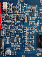
Just copied the Topping pic to Irfanview and magnified it some more there.
With a little more magnification traces combining in and out of phase outputs together at each DAC can be seen. The 100MHz clock can be seen between the DAC outputs and the IV stage inputs (maybe an odd place to put it). Switching power supplies are off to the right. Voltage regulator chips silk-screen marked as being for AVCC left and right channels. Part numbers can be read on some of the chips. However, the bottom area in the pic is a little out of focus so can't see as much there.
- Home
- Source & Line
- Digital Line Level
- ES9038Q2M Board