Mikett, I am glad to read that the lt3042 board is working since I had a dual version of that board and it didn’t exactly work, had already altered the voltage, so couldn’t return it.
Maybe I’ll try again.
I’ll bet the dac sounds good, has been an interesting read...
Maybe I’ll try again.
I’ll bet the dac sounds good, has been an interesting read...
It has to do with the vision and the difficulty. 40 years ago it probably would not have been a problem. This may well be the last round of this hobby and henceforth...gotta pay "real" coin for stuff.
My eyes are getting old too. There are a couple of things that can help quite a lot:
Amazon.com : Carson Optical Pro Series MagniVisor Deluxe Head-Worn LED Lighted Magnifier with 4 Different Lenses (1.5x, 2x, 2.5x, 3x) (CP-60) : Sports & Outdoors
Robot Check
I built most of the small circuits with a headband 2x or 2.5x magnifier. Towards the end, I got one of the 10x long distance microscopes. Wow! When something fits under it and can be evenly lit up, it is incredibly good. Also, later found a dual illuminator to use with it. It may seem pricey, but not necessarily more so than a good pair of eyeglasses with coated lenses these days.
Without visions aids, there is no chance I could see small stuff. It's a blur otherwise. The microscope isn't tall enough to work with a typical circuit board holder, but a using a machinist vise to clamp a PCB by its edges works fine.
The gizmo I showed pictures of earlier is made out of a flexible dial indicator holder. It is super precise and has one thumbscrew adjustable variable axis. I can use it to hold SMT parts for soldering, use it as a micro-positioner, etc. Figuring out how to overcome one's physical limitations is necessary with increasing age.
I also found that I had to grind down and modify small tweezers for handling very small SMT parts. Stock tweezers have tips that aren't finely finished enough and most of them will open and eject a part if squeezed too hard. Those things can be fixed, however.
Last edited:
OK, what about those shaking hands? any ideas for dampers/shock absorbers for those?My eyes are getting old too. There are a couple of things that can help quite a lot:
Amazon.com : Carson Optical Pro Series MagniVisor Deluxe Head-Worn LED Lighted Magnifier with 4 Different Lenses (1.5x, 2x, 2.5x, 3x) (CP-60) : Sports & Outdoors
Robot Check
I built most of the small circuits with a headband 2x or 2.5x magnifier. Towards the end, I got one of the 10x long distance microscopes. Wow! When something fits under it and can be evenly lit up, it is incredibly good. Also, later found a dual illuminator to use with it. It may seem pricey, but not necessarily more so than a good pair of eyeglasses with coated lenses these days.
Without visions aids, there is no chance I could see small stuff. It's a blur otherwise. The microscope isn't tall enough to work with a typical circuit board holder, but a using a machinist vise to clamp a PCB by its edges works fine.
The gizmo I showed pictures of earlier is made out of a flexible dial indicator holder. It is super precise and has one thumbscrew adjustable variable axis. I can use it to hold SMT parts for soldering, use it as a micro-positioner, etc. Figuring out how to overcome one's physical limitations is necessary with increasing age.
I also found that I had to grind down and modify small tweezers for handling very small SMT parts. Stock tweezers have tips that aren't finely finished enough and most of them will open and eject a part if squeezed too hard. Those things can be fixed, however.
Sometimes I am shaky. The micro-positioner helps. Resting my hands and or arms on something close to the work helps too.
Could maybe find or make some padded blocks or adjustable armrests. I have thought about making something to hold the soldering iron and move it in and out, but haven't had to go that far yet.
Could maybe find or make some padded blocks or adjustable armrests. I have thought about making something to hold the soldering iron and move it in and out, but haven't had to go that far yet.
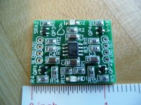
Low Noise LT3042 Linear Regulator Power Supply Board DC Converter Overvoltage | eBay
The above is the link. The board ships with 5V and that is why I initially replaced the 7808 (Ver 1.04) with this power supply. (Ver 1.06) goes directly with the 5V. I tried it and it worked.
To convert the board to 3.3V simply tack a 100K resistor acrosss R1 pad to the ground pad across. This makes for approx 33K paralleled resistance giving 3.3 volts. R1 and R2 are paralleled. It appears the intial designers of the board intended to ship either 3.3 or 5V as assembled.
thanx!
I finished my opamp AVCC today! I used a board with holes and single solder points. I cut a slim part, soldered the opamp on socket in the middle and sticked copper foil left and right side to the opamp as GND, with 2 lines solder dots left free between copper and socket. This gives an easy board and parts can be connected easy to GND.
First distortion measurement was promising - I kept the 390uF polymer caps and just put the new AVCC lines from opa-board to the cap solder points (GND was connected to GND entry of +-15V board terminal and to one of the caps GND pins.
I did a lot of measurements, tried to feed the 1,2V reg by 3,3reg directly or from AVCC, placed a resistor into the line..but as you can see on my measurements I posted before, I had a big distortion peak between 20 and 100 Hz - this is only on left side, right side gives a completely flat distortion line and I could not get rid of it.
At the end I decided to do it exactly as Markw4 did, and replaced the 390uF with 47uF elcos. The left channel peak still was there and distortion on left channel was even a little higher than my 390uF version with 2 seperate regs for AVCC, but sound is somehow more precise in bass, not loosing so much of the deep bass I would have expected.
Overall I can say, the opamp is an improvement soundwise. Regarding my measuremnts I don´t know what is going on with my left channel - I changed output buffer opamp but no impact - maybe something with board analog design or with DAC chip - probably changing to current mode will improve this.... Anybody compared left and right THD and recognized same behaviour?
Last edited:
Regarding the left channel, maybe check both left channel output phases. Also, there is one AVCC pin for the left channel and one for the right. Perhaps the left and right power sources could be switched. If power going in is good, then both output phases coming out should be good, assuming digital inputs are good for both channels. If in voltage mode a mic preamp or maybe a line preamp could probably be used as a signal tracer to tap into each output phase and give each a listen.
Just a quick suggestion regarding AVCC: The guys at Twisted Pear have done several iterations of their circuit, and their customers have sometimes purchased upgrades more than once. There should be a lot of AVCC boards sitting in boxes and drawers somewhere available for this type of usage.
Regarding Twisted Pear, these Q2M DAC chips require much less AVCC current than the PRO version chips. For a Q2M, a dual opamp appears to work fine.
OK, what about those shaking hands? any ideas for dampers/shock absorbers for those?
I have used one of these. takes a while to get used to.
Picked mine up at a yard sale for cheap.
Only just realised what it retails for when trying to find the link...ouch!.
Ergorest - Ergorest Mouse Support - Forearm Support
Regarding the left channel, maybe check both left channel output phases. Also, there is one AVCC pin for the left channel and one for the right. Perhaps the left and right power sources could be switched. If power going in is good, then both output phases coming out should be good, assuming digital inputs are good for both channels. If in voltage mode a mic preamp or maybe a line preamp could probably be used as a signal tracer to tap into each output phase and give each a listen.
I got it! I measured with -4 dB digital attenuation all time before. Now I tried to reduce level and - Bingo! With only 1 dB less (-5dB) the harmonics dropped below 100 dB in a flat line! It seems that left channel is more sensitive to overload than the right. Maybe this can be given as recommendation for all using this DAC board to not drive it with -4dB or higher (in case of analog vol. control). As I use digital volume control via I2S I can live with this. Maybe others could solder an adequate resistor to the volume pot-outs of the board to limit max. level on digital side.
Happy night!
Last edited:

Maybe others could solder an adequate resistor to the volume pot-outs of the board to limit max. level on the digital side.
Ultimately, maybe the best way to handle that is probably in the SRC4392. To prevent intersample over distortion the digital output should be limited to -3.5dB FS (or whatever one chooses, Benchmark uses -3.5dB). The SRC can do that at the same time as doing the upsampling and outputting I2S data to the ES9038Q2M with the Q2M as I2S clock master and its jitter correction off (assuming the SRC4392 can meet the data setup specs of the Q2M, otherwise it may get a little more complicated).
Anyway, I have already tested the first two functions, upsampling and intersample over prevention. For the remaining one, I either need to get a non-disclosure agreement or a friendly programmer with one to set the Q2M into the proper mode. The code for that will necessarily have to be closed whoever does it. For everyone else, it will just have to be treated as a black box.
Last edited:
Hello, you have board 1.04 as me, one question, 7808 is used here to reduce 15V, which is originally used for LPF opamp analog out buffer, onto 8V and then by AMS1117 onto final 3.3V which is used for AVCC chip, and there is no need to have 8V(Ver 1.04) or 5V (ver.1.06) "middle" voltage for any board circuit ? , so would help in SQ to use separate power supply 3.3V, removing AMS and fed it separately... or also i have seen some increasing both capacity from 100uF to 180uF or higher in AVCC circuit to improve SQ, if I have good power supply (dual +/- LT3042 -15V) and i am using it for separate analog output stage (HDAM+DiamondBuffer) and also use this power supply for DAC chip (7808...), would removing AMS and replacing it by separate power supply (for example another single separate 3.3V from 3042) bring any better SQ ? , for reclocking this board i am using AlloReclocker which is fed separately with Rpi3 by Ifi power... so any reason why use separate 3.3V for chip AVCC and increasing capacity if one power suplly is filtered well? thanksLow Noise LT3042 Linear Regulator Power Supply Board DC Converter Overvoltage | eBay
The above is the link. The board ships with 5V and that is why I initially replaced the 7808 (Ver 1.04) with this power supply. (Ver 1.06) goes directly with the 5V. I tried it and it worked.
To convert the board to 3.3V simply tack a 100K resistor acrosss R1 pad to the ground pad across. This makes for approx 33K paralleled resistance giving 3.3 volts. R1 and R2 are paralleled. It appears the intial designers of the board intended to ship either 3.3 or 5V as assembled.
Hi Andora
Using the schematic that xx3stksm presented earlier (Post http://www.diyaudio.com/forums/digital-line-level/314935-es9038q2m-board-18.html#post5336542) - the specific modifications that are needed to get 2V RMS and 0V DC offset at the output are
1. R7, R8, R10, R11 = 0
2. R9 = Rb (Biasing) = 1.58K
3. R12 = Rf (Feedback) = 1.58K
3. C6 = 100uf
If you can get 1.58K resistances - you will have a DC offset of 0V and 2V RMS. I.e. you will not need a coupling cap.
If you want to understand the logic behind what I did - refer to this PDF https://ocw.mit.edu/courses/media-a...g-2011/readings/MITMAS_836S11_read02_bias.pdf
Refer to the formula used for "Inverting Amplifier (DC Coupled)"
-G*Vi + (1+G)Vb = Vo
When we assumeAlso note
- R1 = R3 = Ri = Internal Impedance of DAC = 774 Ohm
- R2 = Rf = Feedback resistance
- R4 = Rb = Biasing Resistor
Plugging all of them in, we get
- G = Rf/Ri
- Vi = AVCC/2 = 1.65V
- Vb = Vi*Rb/(Rb + Ri)
Vi * Rf/Ri = (1 + Rf/Ri)* Vi * Rb / (Rb + Ri)
Solving, we get Rf = Rb
But I could not get exact resistances and soldering was difficult. So I bypassed the existing resistances simply didn't care to get the biasing exact resulting in me having a slight DC offset at the output. Fortunately my preamp doesn't care about it
But if you have well matched 2K resistances laying around - bypass R12 and R9 (8.3K each) with a 2K resistor to make a 1.6K equivalent. That will put you at a gain of 2.07 (1600/774)
Consider this the final analysis.
I am moving on from opamp based I/V stage at this point and going back to transformers.
As an aside - the advantages to this method of I/V areRegards
- Single Opamp
- Existing Layout
- Simpler changes
- Better than Sabre's recommendation since there is no coupling cap at the output
Hello Madds1,
is below circuit correct? R9=R12= 1.58KOhm. Inputs 1 and 2 are I+ and I- outputs from DAC or is there some AVCC/2 offset voltage necessary? Are the caps correct - especially the 390uF?
Attachments
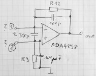
If I reduced R9 and R12 to 1K each, gain would be reduced from 2,0V to 1,3V right? My descrete OPA only permits feedback resistors of up to 1K and I don´t need so much gain anyway in my set-up. As I adjust volume digitally, I could increase resolution though...
Regarding DC offsets and coupling caps. My circuit has no DC offset to speak of and has no coupling cap. That is the nature of current mode with a differential output stage. In addition, I don't have to use special value resistors to make it work. It has excellent sound quality for folks who want to try to optimize that.
EDIT: I edited the first version of this post because I felt kind of frustrated and it didn't sound right. A lot of effort is being expended to offer the best sounding mods. I would hope that's what people would like to have. Technically speaking, going to any trouble to get rid of one output cap is the least of the problems with an unmodified or minimally modified DAC board, which makes it seem not quite rational. If there is something I am not understanding right, please educate me. I would like to know. Thanks for your patience and understanding.
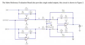
EDIT-2: The circuit xx3stksm originally posted was for a differential output stage with HF filtering. It is recommended by ESS for use after IV conversion on each output phase. The differential stage would then combine the IV outputs into a single-ended output. At that point no output cap should be needed. Changing any of the resistor values to zero or infinity completely changes the function of the circuit. When used properly as a differential output after IV conversion and as ESS recommends, it should do a good job.
EDIT: I edited the first version of this post because I felt kind of frustrated and it didn't sound right. A lot of effort is being expended to offer the best sounding mods. I would hope that's what people would like to have. Technically speaking, going to any trouble to get rid of one output cap is the least of the problems with an unmodified or minimally modified DAC board, which makes it seem not quite rational. If there is something I am not understanding right, please educate me. I would like to know. Thanks for your patience and understanding.
EDIT-2: The circuit xx3stksm originally posted was for a differential output stage with HF filtering. It is recommended by ESS for use after IV conversion on each output phase. The differential stage would then combine the IV outputs into a single-ended output. At that point no output cap should be needed. Changing any of the resistor values to zero or infinity completely changes the function of the circuit. When used properly as a differential output after IV conversion and as ESS recommends, it should do a good job.
Last edited:
Attached below is the full circuit as recommended by ESS. Anybody recognize the differential output part? Obviously, the parts values are different from the other proposed circuit and have been scaled for optimal SQ in its intended role.
Attachments
Last edited:
- Home
- Source & Line
- Digital Line Level
- ES9038Q2M Board