You're confusing this with a different RC. My RC is 47p/3.3k and goes in a different position, as you can see on the schematic.
EDIT: Or maybe I just misunderstood the last few posts.
A 47p/220R RC across the gate and drain is meant to damp the parasitic inductance of the MOSFET, which is a much different issue than my 47p/3.3k is meant to address, which is the T5/M1 feedback loop. While both issues can reduce stability, they need to be addressed separately. I think it is unlikely the 47p/3.3k RC will help if M1 is oscillating by itself, but given that it's gate is driven by an unsaturated BJT collector, this scenario is unlikely.
Last edited:
Kean,
You confused me somewhat with your post!! What issue requires addressing when one of them, the Gate Drain snubber, damps out any oscillation (self or otherwise) arising either from it's internal structure, and should also damp the controlling transistor T5 should it oscillate.
I believe the principal compensation should be addressed to the VAS, that is T3. The secondary loop, comprised of T5 and the upper nmos, is not too worrisome because the (open) loop gain is set by the 100k from base to collector and there is in fact a highish Ciss on the mosfet (2-3nF) gate to source which would load down the loop gain of T5 at high frequencies. The Pass Aleph, from which this dynamic CCS is taken directly and with no change has no such snubber, possibly because it works with constrained OLG on T5 and IRF mosfets which have low Ciss and low gm.
The fundamental stability issue of this amp lies within with the AKSA/Lender preamp front end which drives the output stage. I've not used lag compensation - collector to base on the VAS device - I've chosen to get sneaky with it using shunt compensation (collector of VAS T3 to ground) and phase lead (output to fb node), as you alluded.
The amp is evidently stable in X's tests, and while compensation is an art and relies on careful experiments, at least for me, it seems to be a doddle with the ALPHA. Oscillations at 5MHz from T5 were a surprise to me; but I would be surprised that it would be an issue if NP has not added a snubber from collector to base. I did notice one NP variant which replaced the 100k with a 10nF cap; that would pull back gain to almost nothing at 1MHz, and that may have been added after the effect with higher gm mosfets. It does occur that using a slow transistor for T5 might also be a good option, say something like a BD139, I assume it's a slow device because I've never been able to find its ft in my datasheets!
Again, thank you for your post. The more issues we uncover and address the better the amplifier becomes.......
Hugh
Last edited:
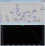
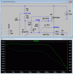
If you think about that chart you can see that the 5MHz resonance is about 20db down from the gain of the amp. This would make it hard to notice on an oscilloscope screen, maybe invisible depending on the Q.
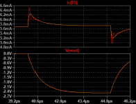
So it might be there, just no one has noticed it. Here is a picture showing the resonance with and without my snubber. Note that there is no perceptible change in the square wave shape. It's probable this resonance exists, it just doesn't show up on the scope. So I suggest to try out the snubber and see how it sounds.
BTW, a 220p/47R G-D snubber actually worsens the resonance rather than reducing it.
Attachments
Last edited:
BTW, a 220p/47R G-D snubber actually worsens the resonance rather than reducing it.
Can you show me this on a graph? Why would Cordell suggest this if it were not effective?
HD
Thanks for the simulation!
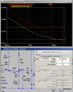
I checked out the feedback node capacitance. All the Miller path components need to be grouped together, so I just added R19 as an easy way to measure the feedback node current. The red line is the feedback node capacitance, the yellow line is the capacitance of just the transistor base. It's about 1.6pF. I used my own models just to rule out a model issue.
So the idea that the phase lead capacitor is compensating for a capacitance shunting the feedback node is untenable. It was a good use of insight and lateral thinking, but it was not to be.
Note that both C6 and C9 form the phase lead compensation. They participate nearly equally according to their ratio.
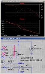
In the second image I've added a 47p+3.3k C10/R22 RC network to get rid of the resonance at 5MHz. This resonance may be interacting with the phase lead compensation and exacerbating audible effects. Who knows.
When I mention Requivalent and Cequivalent, I suppose that these two elements are the equivalent of what would be seen towards the base terminal of the transistor plus the joint action of some peripheral components that are connected (in one way or another) to the junction point of the resistors of the feedback network (junction point between R6 and R7).
Seeing the scheme that you have gently loaded, Requivalent and Cequivalent would be represented by: base terminal of T2 (which defines two parasitic capacitances: one towards BE and another towards BC) plus all the components that end in one way or another towards the terminal base of T2 (including the action of T3 on the parameters of Requivalent and Cequivalent).
Thus, the Cequivalent should be higher than those 1.6 pF. You said: "The yellow line is the capacitance of just the transistor base".
Regards
Last edited:
In most situations the gate is driven by a low impedance, which allows the gate inductance to define the drive impedance. In this case the gate is driven by a high impedance BJT collector, which DOES effectively block the colpitts oscillator parasitic circuit.
The other thing is, T5 and M1 have their own feedback loop separate from the amp itself. This feedback loop is not unstable, but it's not fully compensated which is why it resonates. This feedback loop is destabilized by Cgd, so the G-D RC has an effect on it that it does not have on a normal emitter-driven MOSFET without local feedback.
Cordell's RC is correct for MOSFETs driven by BJTs or an otherwise low impedance.
Can't make a graph right now, now time.
Thus, the Cequivalent should be higher than those 1.6 pF. You said: "The yellow line is the capacitance of just the transistor base".
Regards
This amount of capacitance matches with the KSA992 datasheet. Cbe doesn't do anything because 1: it is bootstrapped by the emitter - 2: the LTP is lightly loaded.
All the other components in the feedback network besides T2 and the feedback shunt resistor all come from a node where the output voltage makes up the bulk of the signal, and the differences between the nodes are secondary to that.
Specifically, the output stage is a buffer, and the feedback is taken from either the input of the buffer or the output of the buffer. So the feedback signal is taken partly from both points according to the ratio of impedance between the two sets of feedback components.
So assuming the Cequivalent doesn't come from T2 or the feedback shunt resistor, we also know it can't come from C6 because that is the capacitor that is in theory compensating for it.
That leaves C9, C5 and R16.
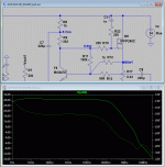
The yellow trace is the normal capacitance plot, the red trace has the real component of the complex impedance removed just in case it is swamped by a resistive component (which is apparently the case). The impedance only behaves like a real capacitor after 10MHz - 20pF, about the value of C9 plus the capacitance of T2. The orange line is a 220pF capacitor.
Also I must eat my words about Cordell's RC. I got the curves mixed up when I investigated it. The red trace is without it, the orange trace is with. It does reduce the resonance, but it's not as efficient as my RC as it more than doubles the load on T5.
Attachments
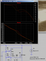
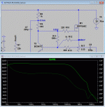
Well, it turns out in that last image I was using the wrong R value in the RC. Here it is with the standard 220p+47R RC. It does get worse, just like I said. You can use different values and get somewhat better results, but it's a solution to a different problem than the one we have.
Attachments

Keantoken,
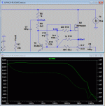
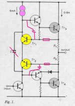
You have the snubber in the wrong position in the last test - see attached drawing.
You could also try varying the values of the snubber R & C. I suspect that the 47ohm resistor should be a bit lower in value (15 .. 33). I'll be really interested in the result.
Paul Bysouth
You have the snubber in the wrong position in the last test - see attached drawing.
You could also try varying the values of the snubber R & C. I suspect that the 47ohm resistor should be a bit lower in value (15 .. 33). I'll be really interested in the result.
Paul Bysouth
Attachments
I see two possibilities if we assume that Cequivalent is the correct explanation.
The first is that just like in Diego's simulation, the output bandwidth will be flat to a higher frequency with C113 rather than without.
The second is that Vout will have the same AC response as the base of V102, when C113 is at the right value, rather than the AC responses being different.
If either of these are not the case, then it does not look good for the Cequivalent theory.
These two possibilities would be true, if the feedback network is analyzed acting alone and separately from the rest of the circuit, in the same way as a perfectly compensated oscilloscope probe would do. Now, when that feedback network operates with the rest of the amplifier, that same network will continue to act as well and the high frequency attenuation will be caused only by the own and inevitable limitation of the active elements that are linked with her.
In addition, network compensation will only be possible if it simultaneously complies with the condition to guarantee the necessary stability margin for any amplifier (a fact that I believe could not be met in most cases).
Anyway, I think the subject is still much more complex than we can suppose. It would be innocent to think that all capacitors (those formed in the active elements) will remain static at all frequencies and, even, under different signal levels. The most optimal compensation could be given, at the most, only in a limited range of levels and in a limited range of frequencies. Being objective, I doubt even my own theory, although it does not seem crazy. Being objective and sincere, I also doubt that the spatial aspect can be improved by a small adjustment of the value of that capacitor, a subjective fact that should be tested to see if it really exists and can be attributed to that single change 😕.
Regards
The values of the snubber 220p+47R don't seem to be optimal,
I get better result with 1n+220R
But the snubber solution of Kean gives the best suppression.
Here are the three snubber options compared:
Non - 1n+220R - Kean
I get better result with 1n+220R
But the snubber solution of Kean gives the best suppression.
Here are the three snubber options compared:
Non - 1n+220R - Kean
Attachments
Last edited:
Thank you Danny. How about a four option; 3k3 from base of T5 to 47pF end connected to the GATE of M1, not to the left of R10, but on the right?
I agree that the third option seems to remove the inflexion point on the phase curve very well.
I believe that there should be a snubber from gate to drain on the pmos, that is, no change.
Thanks for input from all the experts, slowly we are getting to the nub of it.
HD
I agree that the third option seems to remove the inflexion point on the phase curve very well.
I believe that there should be a snubber from gate to drain on the pmos, that is, no change.
Thanks for input from all the experts, slowly we are getting to the nub of it.
HD
Many thanks..... I'm not sure that taking the snubber to the gate directly is the best option; I was trying to combine snubbing on both T5 and the nmos. The fact is that when you use high power, high gm mosfets that 47R-220pF from gate to drain scotches self-oscillation in these devices; any resonance in T5/M1 at 5MHz is academic because the gain of the amp will well below 0dB and positive fb cannot produce destructive oscillation. Looking at this logically, it would seem that NP does not use a snubber across the C/B of T5, and Cordell recommends a snubber at gate to drain, I'm inclined to leave the design exactly as it is...... unless Kean, Diego, Maty, or Paul can come up with a very good reason there is no requirement for two independent snubbers here.
Many thanks. It does seem that Nelson got it right, but using bigger, more transconductance mosfets might just change things a little.......
HD
Many thanks. It does seem that Nelson got it right, but using bigger, more transconductance mosfets might just change things a little.......
HD
Last edited:
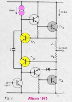
The output stage of the Alpha amplifier is similar to the top half of an Allison bias type output stage (published by Allison in Wireless World in 1975 - see Fig1), which I have drawn in Fig3 showing only the top half of the output stage and ignoring the Aleph control.
This part of the amplifier has a two transistor feedback loop created by Q1 and M1, and it will have a reasonably high loop gain (*). There is the possibility that this loop may be unstable or only marginally stable, so it may need some form of compensation.
Fig2 shows how I would normally compensate an Allison bias circuit, and so applying this to Fig3, R4 and C1 would be used to ensure the Q1,M1 loop is stable (the Yellow box). I have no idea what the R4,C1 values should be, but 47pF would probably be a good starting point.
Normally irf240 type mosfets don't need a snubber (the Green box), but is probably a good idea. The high Gm type mosfets (Fairchild FQA and IXYS types) probably need one. When Hugh started experimenting with using FQA mosfets he managed to destroy a few before the snubber scheme was perfected (but none since as far as I know).
* I've frequently, over about 10 years, tried to think of how to determine the loop gain of an Allison type circuit using LTspice - does anyone have any ideas?
So I suspect that the Alpha should have both the Yellow and Green box types of compensation, but that the Green box snubber would only be needed for the larger FQA/IXYS type mosfets. Maybe Q1 should be a slow transistor (eg BD139) given that M1 will be much faster. Does anyone have any ideas on how to determine the optimum values?
On an associated point, both Hugh and I use low power gate resistors for output mosfets (usually 1/8watt thin film Stackpole rncp1206). If the mosfet does decide to burst into oscillation, then it will draw a lot of gate current, which will cause the gate resistor (ie Rg) to destroy itself (usually open circuit) and hence protect the rest of the amplifier.
regards,
Paul Bysouth
Attachments
Talking about snubbers, your words (class AB SAKSA 85):
New SAKSA amp - Amplifiers & Pre-Amps - StereoNET
New SAKSA amp - Amplifiers & Pre-Amps - StereoNET
Maybe the SAKSA 85 -class AB amplifier with H2 predominant- is better idea to low sensitivity speakers like mine I think. And it is not a stove lit in Mediterranean summer. ALPHA 20: almost 150 watts.1. Four stage Class AB bipolar/mosfet amplifier with diff pair input, Lender SE voltage amp, SE impedance transformer (constant power, single bipolar), bipolar bootstrap drive, complementary 2x280W mosfet output stage.
2. Front end is a LTP with modified stage source. This offers outstanding offset control, zero thump turn-on and flexible input impedance. This stage has predominating H2 and H4 harmonics.
3. The voltage amplifier (VAS) is a fast, high beta device operating at 1.5mA. It is driven both at base and emitter. This delivers accuracy, low phase shift, and very low distortion. This is the heart of the amp.
4. An impedance transformer, an emitter follower, takes the VAS output at very small drive and turns it into a low impedance output stage to drive the outputs. This device operates at constant current and voltage, so has 100% linearity. Strong drive is needed for the hungry gates on the push pull output stage.
5. In the first three stages the signal is single ended. In the output stage we split it to achieve PP operation with Class AB efficiency. I use high power output mosfets with great care to prevent self-oscillation, which destroys most mosfet in the field. Careful use of gate stoppers and snubbers from gate to drain make this a very, very stable and powerful output stage that I use in many amps these days. These devices have only become available in the last 15 years, and use up to 1040W monsters in my larger amps. You cannot break them; they are used in electric vehicles, for example, and ideal for audio as they have very, very high transconductance which depresses the usual compressive distortions of Class AB amps...
Last edited:
Well Maty my words thrown in my face!
Now everyone knows how AKSA feels!
Paul explained my massacres battling smoke from large trench mosfets, what saved me was a 1984 white paper on protecting mosfets. The 47R/220pF snubber prevents smoking mosfets.
When you work with bootstraps you see that self inductance of the caps raises their impedance beyond 500KHz. The bootstraps loses effectively and therefore the 5MHz glitch Kean uncovered is lost in the bootstrap failure beyond 500KHz.
Yes Maty the AB SAKSA 85 would suit your hot climate. It's not a Class A but it is a very good Class AB.
HD
When you work with bootstraps you see that self inductance of the caps raises their impedance beyond 500KHz. The bootstraps loses effectively and therefore the 5MHz glitch Kean uncovered is lost in the bootstrap failure beyond 500KHz.
In order for the bootstrap to behave differently than in the simulation the capacitor's inductance needs to be large enough to overcome the bootstrap resistance. To investigate this we can take the smallest bootstrap resistor of 1k and see how much inductance it takes to increase it's impedance at 5MHz.
That would be
L = Z/(2piF) or
1k/(6.28*5MHz) = 32uH
The capacitor inductance is probably no more than 22nH.
A general rule of thumb for resistors is that their impedance approaches that of free air, 300 ohms, as frequency increases. Resistors under 300 ohms tend to be inductive, larger resistors tend to be capacitive. A 1k resistor is close enough to 300 ohms that it will still be a resistor well above the ULGF of this amplifier.
So I accept the possibility that this resonance does not show up in a real amplifier, but if that is so the boostrap inductance can't explain why. I've also shown that we probably don't know whether it does or not, due to the fact that it's not apparent in typical measurements. Furthermore, I know the models used in simulation to be reasonably accurate.
So I suggest that someone at least try out the 3.3k+47p RC, maybe even measure the resonance directly.
- Home
- Amplifiers
- Solid State
- Aksa Lender P-MOS Hybrid Aleph (ALPHA) Amplifier