Andrew, if you read the ESP website description text, you'd have seen a discussion on the suggested bias level in current terms, which I have translated for either way of expressing the result as a current or a voltage measured across a given Re value. This is far more common parlance than EE speak on this forum. Read the article before firing off dismissive criticism at me from the hip and notice that I have done little more than restate the designer's suggestions.....The optimal bias for ClassAB is a VOLTAGE.
Sergiog has it correct....Optimal ClassAB is to minimise crossover distortion.
The advice being given by Ian F is nonsense
For this design, an "optimal" bias is obviously the last thing on Rod Elliott's and most constructors minds when building their own P3a. The amplifier happens to sound much better subjectively at 50 mV across Re than with 5, as would suit a CFP output stage biased "optimally" for lowest THD. It should have seemed an odd high bias figure when you read sergiog's post where the 50mV figure arose.
This high bias level accords with CFP design amplifiers from Hitachi and Sony, to name a couple of manufacturers, back in the 1970-80 period. As I recall, most of these models ran quite hot with between 50 and 100 mA bias current but were well liked for the sound. Yes, I did say bias current again because this is class AB and not optimally biased class B, as Self puts it. The very reason for this project's popularity is perceived SQ and you will note that Rod experimented with a wide range of currents, as I mentioned. If you go back to the OP, you'll find Sakis discussed the same observations with different current levels in his build, as the basis of comparison with many commercial products that come his way as a repairer.
After all, what's the point of building an optimally biased amplifier that sounds poor by comparison? 🙂
I must admit that all Ian said about SQ versus bias is correct. I used P3A with optimal bias at around 10mV across 0R33 for a long time. Than I wanted to experiment a little and changed it to 40mV. I was surprised that the sound was much more to my taste, more exciting, detailed, dynamic and vivid. It seems that higher bias serves well CFP designs. I am currently using P3A with PGA2310 volume controller and the sound is "prima".
ATTENTION.
I found a mistake in this pcb.
Green led is in opposite direction.
Hello Thimios sir
I found some error in this layout, I try to correct it, is this modification is ok, Is R15 & C7 connection is right.I think C7 should connect o/p through R15.Please correct if I wrong.
Attachments
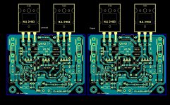
AlexMM pcb is good! It's not necessary to follow the sequence of R15 and C7 from the schematic. They can change places. The sequence in the AlexMM pcb is dictated by the space and layout of components on the pcb.
But Thimios was right about orientation of LED. It should be reversed compared to what is shown on the top side of pcb.
But Thimios was right about orientation of LED. It should be reversed compared to what is shown on the top side of pcb.
Last edited:
Hello Thimios sir
I found some error in this layout, I try to correct it, is this modification is ok, Is R15 & C7 connection is right.I think C7 should connect o/p through R15.Please correct if I wrong.
you could also take a look at superR layout.
AlexMM pcb is good! It's not necessary to follow the sequence of R15 and C7 from the schematic. They can change places. The sequence in the AlexMM pcb is dictated by the space and layout of components on the pcb.
But Thimios was right about the orientation of LED. It should be reversed compared to what is shown on the top side of PCB.
Hello ivanlukic
thanks for reply, What about Q9, Alexmm uses BD139 But as per Rod Elliott sir It should be BC546.
It's not a problem that AlexMM pcb uses BD139 as Vbe multiplier. BC546 has higher hfe and theoretically can correct bias faster than BD139. That's the reason why some APEX circuits use Darlington transistor for Vbe multiplier.
But in this case output stage is CFP (Sziklai) configured. Ian Finch claims that if Vbe multiplier is placed directly on the driver transistor itself it can overcompensate bias. Therefore using lower hfe transistor like BD139 can even be beneficial.
But in this case output stage is CFP (Sziklai) configured. Ian Finch claims that if Vbe multiplier is placed directly on the driver transistor itself it can overcompensate bias. Therefore using lower hfe transistor like BD139 can even be beneficial.
hi, sorry but after a few months I finished the ampli (sound good) came a problem I noticed that turning off the amp the led delayed to shut off and the boomp at the ignition was weaker. Checked the power and i I have noticed that the positive branch is always charged, after a few hours I still have 7V, the negative branch is OK (0.00V). From what may depend, the active components I have used are: Q4 = MJE15035, Q5 = MJE15034, Q7 = MJL21193. I changed all the power components but nothing has changed. Anyway currently the amp works well and no kind of noise. Someone can get away from what may depend. Regards Gilardi Italy
Check your power supply if charging and discharging time is equal, the problem could exist there.
hi,When I turn on the amp the power supply immediately marks the +/- 34V and the amplifier works well immediately. When I turn it off only the negative rail goes to 0.00V the positive rail goes immediately to + 22V and then after 3 hours it still marks + 7V. The only thing I changed in this last period is the bias from 50mV / 0.66ohm to 22mV.Regards Gilardi
many dual polarity circuits do not draw equal currents.
During shut down this unequal current draw can become extreme.
At some point the current draw on one polarity can drop to near zero.
This appears to be happening to your circuit.
You can force the current to be higher by adding a load resistor to that supply line.
Or you can add a 2pole relay that is normally closed. This goes open during operation and closes at shut down. That closing action can bring in a discharging resistor on each supply line.
and then after 3 hours it still marks + 7V.i
This behaviour seems pretty strange that is quite a very long time to discharge. My P3A discharges for just a few secs just after powering off.
Indeed a bleeder resistance would take care of this.
I think it is better to have all caps gone discharged at power off, because who knows what can happen when powering on just after going off. The risk is, the caps left charged will discharge in components that cannot survive it.
A safe way is, bleeder resistances at the PSU outputs.
I think it is better to have all caps gone discharged at power off, because who knows what can happen when powering on just after going off. The risk is, the caps left charged will discharge in components that cannot survive it.
A safe way is, bleeder resistances at the PSU outputs.
Sorry but I forgot to add that disconnecting the + pole of speaker goes immediately to 0.00V. Sorry again
P3A PCB layout
Hi all,
I started to build SARA than and paused, thinking to start with a smaller one.
Buying P3A from ESP, seems to be costly(26$) for me.
Reading many P3A posts, found few PCB designs and confused to choose one.
Can anyone suggest & provide a good PCB layout (possibly a pdf file)?
Thanks in advance.
Edison C.
Hi Prasi. What is this?you could also take a look at superR layout.
Ok I see,isn't good ,Vbe mult.must be in thermal contact with the VAS not with the outputs.
Last edited:
Do you have them?
I can find the below only..
http://www.diyaudio.com/forums/solid-state/201446-rod-elliot-p3a-layout-critics-9.html#post2815857
I can find the below only..
http://www.diyaudio.com/forums/solid-state/201446-rod-elliot-p3a-layout-critics-9.html#post2815857
Do you have them?
I can find the below only..
http://www.diyaudio.com/forums/solid-state/201446-rod-elliot-p3a-layout-critics-9.html#post2815857
unfortunately not
- Home
- Amplifiers
- Solid State
- P3A Comparison table ( long .... )