To get more output power you can try paralleling more output FETs. The threshold voltages are rarely close enough to parallel at DC but AC paralleling works fine in my experience - you need to duplicate the output cap too when you add the extra MOSFET.
Ooooh, this is an interesting idea, so the idea is to double the mosfet and output caps by making two mosfets in parallel and Making two of each output cap locations also in parallel?
I can try this first as I have the spare mosfets and caps.
Let's see how this works and then try the full desktop variant make over
Thanks you both for the tips!
Ooooh, this is an interesting idea, so the idea is to double the mosfet and output caps by making two mosfets in parallel and Making two of each output cap locations also in parallel?
Yes you duplicate the input and output resistors along with the output cap (no need for extra output biassing/loading resistor). You join at the input side of the gate resistor and again at the output side of the output cap.
I've done experiments with such an approach and the two transistors share the current well in classA so you do in fact get twice the output current capability, along with spreading out the dissipation between two (or more) transistors. In fact I've tried this with 5 paralleled transistors (pic of prototype on my blog).
Output transistor transconductance goes down with increased temp so we do want to run our FETs as cool as possible 😎
Ok got it, and for this board, the input resistors are the R1s and the output resistors are the RLs?
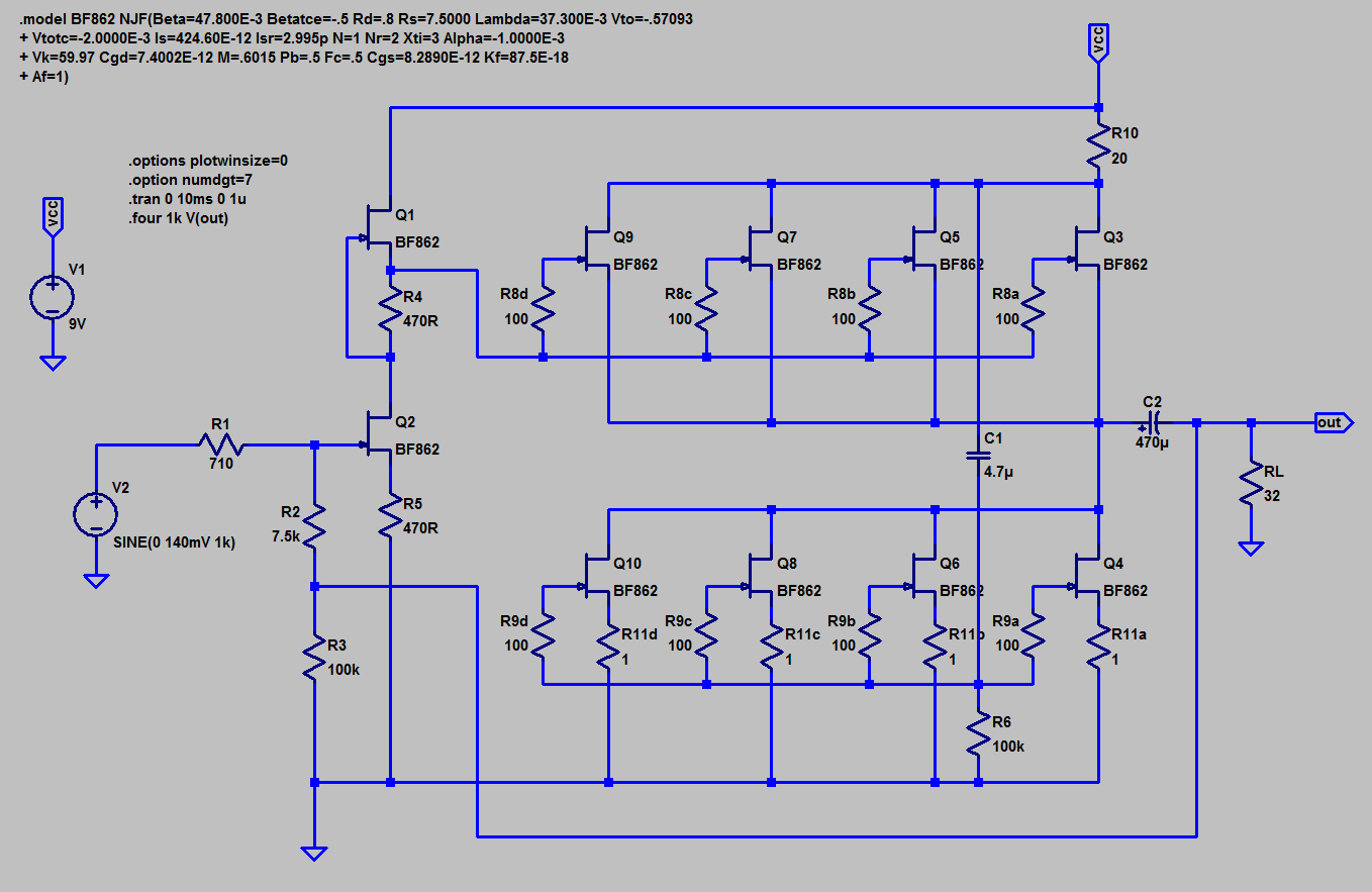
Looking at X's original schematic in the first post of this thread, the input R is R6 and the output resistor is R7. So to duplicate is R6, M1, R7 and C2.
RL could be there to indicate a load (for simulation). Don't duplicate that but a 'pull-down' resistor isn't a bad idea to pre-charge the output cap(s). It should be 10k or so if you want to include it.
RL could be there to indicate a load (for simulation). Don't duplicate that but a 'pull-down' resistor isn't a bad idea to pre-charge the output cap(s). It should be 10k or so if you want to include it.
Looking at X's original schematic in the first post of this thread, the input R is R6 and the output resistor is R7. So to duplicate is R6, M1, R7 and C2.
RL could be there to indicate a load (for simulation). Don't duplicate that but a 'pull-down' resistor isn't a bad idea to pre-charge the output cap(s). It should be 10k or so if you want to include it.
Thank you for the clarification! Wow I am embarrassed to be way off... and there are only 8 resistors to choose from. Lol. I guess 15yrs doing project management straight right after school does take a big toll on my EE knowledge!!!
I have indeed done this and used 8 JFETs for the output and CCS. Matching them becomes important otherwise you have a choir with a few people singing off-key.
http://www.diyaudio.com/forums/head...f862-based-se-class-headamp-without-heat.html
Given a choice of if you can handle the current with a single device, you should do that rather than multiple devices that need matching. This was advice given by AKSA, and I think it is sage advice.
I have simulated a desktop amp using a pair of ZVN4306's but in the end opted to use a single IRF610 - glad I did.
Looking at X's original schematic in the first post of this thread, the input R is R6 and the output resistor is R7. So to duplicate is R6, M1, R7 and C2.
RL could be there to indicate a load (for simulation). Don't duplicate that but a 'pull-down' resistor isn't a bad idea to pre-charge the output cap(s). It should be 10k or so if you want to include it.
And one more questions, for R6, R7 and C2, do they have to duplicate by pairs or just get the equivalent values by a single component works?
PSU
I may look at using a spare laptop 12V, and see what the ripple looks like. Is the step up custom made or commercially bought?
Thank you
It might work but depends on how much line AC ripple gets through. It is switched so that is good for cutting out mains 50Hz ripple, but what is switching frequency? I use a 1.2MHz DC step up after a 12v 3a SMPS PSU.
I may look at using a spare laptop 12V, and see what the ripple looks like. Is the step up custom made or commercially bought?
Thank you
I have indeed done this and used 8 JFETs for the output and CCS. Matching them becomes important otherwise you have a choir with a few people singing off-key.
http://www.diyaudio.com/forums/head...f862-based-se-class-headamp-without-heat.html
Given a choice of if you can handle the current with a single device, you should do that rather than multiple devices that need matching. This was advice given by AKSA, and I think it is sage advice.
I have simulated a desktop amp using a pair of ZVN4306's but in the end opted to use a single IRF610 - glad I did.
This looks very interesting but I am sure it'll be beyond my capability... quoting Homer Simpson, "I am just trying to get into Heaven, not running for Jesus!" Haha
Given a choice of if you can handle the current with a single device, you should do that rather than multiple devices that need matching. This was advice given by AKSA, and I think it is sage advice.
I rather suspect Hugh (AKSA) was assuming DC paralleling - if you parallel DC coupled then threshold voltage matching becomes mandatory. However I've found its not an issue with AC paralleling in an amp which is operating in classA. ClassAB may well be a different matter.
My guess would be IRF610 has lower gm than a number of paralleled smaller devices. But I haven't examined the DS yet - I shall go and do so 🙂I have simulated a desktop amp using a pair of ZVN4306's but in the end opted to use a single IRF610 - glad I did.
@babysupra - sorry can't understand your most recent question 'duplicate by pairs' ?
Last edited:
@babysupra - sorry can't understand your most recent question 'duplicate by pairs' ?
Take R6 for example, its 47R stock, do I need to use two 47R in series (how to series a pair of smd resistors? Lol) or instead I use a single smd resistor in the 94R range (if this exist)
R6's value stays as it is, you can say with two output transistors there will be R6a M1a R7a and C2a, then R6b M2b R7b and C2b. All values the same as in the original.
R6's value stays as it is, you can say with two output transistors there will be R6a M1a R7a and C2a, then R6b M2b R7b and C2b. All values the same as in the original.
Now I am more confused, on pcb there are two channels, labeled A and B, so in stock configuration, there are already one mosfet for each channel, thus M1a and M1b each has one mosfet. And I thought you meant to parallel two mosfet at M1a and two mosfet at M1b, so total of 4 mosfet. And then to support this 4 mosfet configuration I need to "double" up on R6, R7 and C2, no?
Last edited:
Ah I'd not examined the PCB - it wasn't my intention to further confuse you. So let's call the existing output FETs M1a and M1b, you'll need M1aa and M1ba as two new FETs.
You are not paralleling the individual FETs you are paralleling two 4-component circuits which include 2 resistors, a FET and a cap.
Maybe a drawing is best but my screen capture program isn't working and creating a .xps from LTSpice gives an error when trying to attach here. Can you view LTSpice files?
<later> Got screen capture working again 😀
Attachments
Last edited:
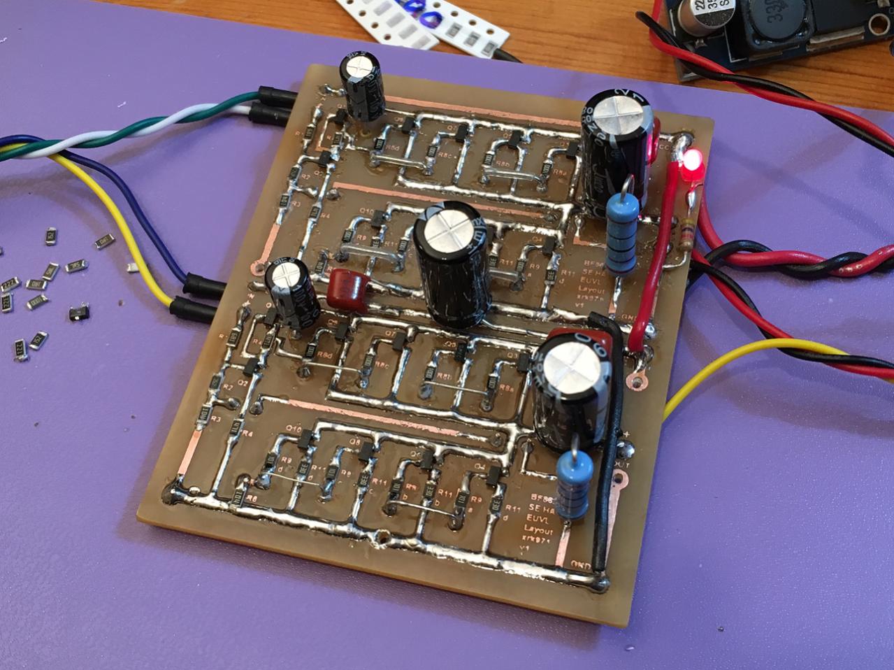
Haven't had more time to listen to it yet, but here's a pic. Ignore the two KZ hanging off horizontally - couldn't find a way to connect them so they didn't make the cut. next time 😉

Now I am more confused, on pcb there are two channels, labeled A and B, so in stock configuration, there are already one mosfet for each channel, thus M1a and M1b each has one mosfet. And I thought you meant to parallel two mosfet at M1a and two mosfet at M1b, so total of 4 mosfet. And then to support this 4 mosfet configuration I need to "double" up on R6, R7 and C2, no?
I don't know why you continue to pursue the parallel MOSFET path. There is no room on the board for it and using a single IRF610 is superior and gives more than enough current as those are rated very high amperage relative to ZVN4306. You should just follow the schematic I gave you earlier for the desktop IRF610 amp if you want to just modify the current board. If you want to make a new board with parallel small MOSFETs that's fine - but it needs to be simulated and not just doubled up like Abraxalito shows. There are heat dissipation issues and distortion balancing via DC settings with the overall resistor network. It's not something you just change - like cap rolling. You are talking about the topology and the MOSFET and JFET operation points being modified. Has to be simulated if you want any chance of success.
I don't know why you continue to pursue the parallel MOSFET path. There is no room on the board for it and using a single IRF610 is superior and gives more than enough current as those are rated very high amperage relative to ZVN4306. You should just follow the schematic I gave you earlier for the desktop IRF610 amp if you want to just modify the current board. If you want to make a new board with parallel small MOSFETs that's fine - but it needs to be simulated and not just doubled up like Abraxalito shows. There are heat dissipation issues and distortion balancing via DC settings with the overall resistor network. It's not something you just change - like cap rolling. You are talking about the topology and the MOSFET and JFET operation points being modified. Has to be simulated if you want any chance of success.
Hi X, ya I misunderstood earlier, I thought what he said was something simple like doubling up components at M1, R6, R7, and C2, didn't realize he meant adding two new paths. Yea that's beyond my capability, back to your desktop variant build. Good learning tho. And sorry for the confusion
... using a single IRF610 is superior and gives more than enough current as those are rated very high amperage relative to ZVN4306.
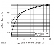
I did go look at the plots for the IRF610 and sure enough, its transconductance is considerably lower than the FET in the current schematic (ZVN4306). Higher transconductance translates to real-world benefits - lower distortion and also lower output impedance. An open loop amp has no reduction of Zout due to loop feedback so transconductance is more of an issue without global feedback being applied.
I've attached the IRF610's relevant plot - the slope of the lower curve gives the gm (transconductance) - for a typical bias current of 30-60mA the gm is in the region of 150mS which gives an output impedance around 6ohms.
Attachments
Haven't had more time to listen to it yet, but here's a pic. Ignore the two KZ hanging off horizontally - couldn't find a way to connect them so they didn't make the cut. next time 😉
Looks like a Game of Thrones iron capacitor mini throne. 🙂
I just placed another order with Mouser for $150 worth of caps. When using premium caps on these amps, the costs add up quick. I really like the combo of dual 1000uF 16v OSCONs plus 10uF 35v Silmic II's. These OSCONs are $2ea x 4 is $8 in caps - the single most expensive set of components. But boy, do they deliver in the bass department with combined 8mOhm ESR when run in parallel. Even driving 14ohm IEM's, the frequency response reaches to 11Hz for -0.5dB point. The 10uF Silmic takes over above 1kHz for astonishing mids and highs. I hear no improvement with a film bypass here.
- Home
- Group Buys
- xrk971 Pocket Class A Headamp GB