Q1,2 5 7 6 are all inside the cascodes.
Thus lower voltage transistors can be utilised.
BC550/560 are 45Vce0 and will do the job, but I recommend using C grade and match them. Leach gives guidance.
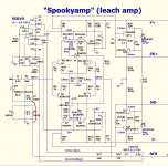
The feedback leg from R33 is connected to the wrong node. It should not be connected to Power Ground. It should be measuring the input signal at the Signal Return, where Vin is connected. Again worth going back and reading Leach.
Thus lower voltage transistors can be utilised.
BC550/560 are 45Vce0 and will do the job, but I recommend using C grade and match them. Leach gives guidance.
The feedback leg from R33 is connected to the wrong node. It should not be connected to Power Ground. It should be measuring the input signal at the Signal Return, where Vin is connected. Again worth going back and reading Leach.
Last edited:
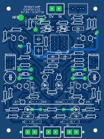
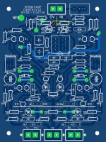
Thanks Andrew, I thought this were a working schematic. Can someone perhaps confirm if this version is ok ? I think this is ver 1.2 of the Spooky.😕
Thanks
Thanks
In my layout the connection point of the NFB network is correct. I noticed this when laying out the board and took the liberty of correcting it. Spooky v1.2 is verified to work.
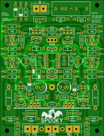
Those images are ostripper's artwork, not mine. My layout is intended for board house production, not home etching, just so you are aware. I'm pretty sure I posted files for the boards, I will look to see if I can link to them. If not I can try to repost them.
Thanks Jason , Much appreciated !🙂
Apparently R23/R24 which is 6.8k apparently has to change. Can you perhaps help with values when the rails voltages are +-70V.
Thanks
Apparently R23/R24 which is 6.8k apparently has to change. Can you perhaps help with values when the rails voltages are +-70V.
Thanks
Last edited:
But Andrew is right - R33 has to be connected to the lifted ground (where R2, C2 are connected), not the power ground. Same thing in the layout. I recommend to connect it the right way, just placing the resistor somehow over the parts, if you already have the boards. Otherwise - easy to correct the layout before etching / manufacturing.
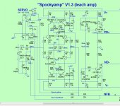
Val, yes I have seen Andrew is correct after looking at the diagram of the V1.3 and V2. Thanks for that Andrew. Val does this look Ok. The red is the cut traces and the yellow is the new connections. I have not yet etched the boards, just now finished sourcing spares. Can you plse help Val.
Attachments
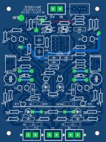
Spooky IPS Files
Attached. Included the 'Cheapskate' files as well that limit the maximum dimensions to 100mm to get better pricing from the discount board houses.
Attached. Included the 'Cheapskate' files as well that limit the maximum dimensions to 100mm to get better pricing from the discount board houses.
Attachments
Val, yes I have seen Andrew is correct after looking at the diagram of the V1.3 and V2. Thanks for that Andrew. Val does this look Ok. The red is the cut traces and the yellow is the new connections. I have not yet etched the boards, just now finished sourcing spares. Can you plse help Val.
Hi Jan, not exactly )
You just need to cut R33 from the power ground and connect it to R2.
All other connections have to stay as they are.
Jason's layout has R33 connected the right way.
Val,OK, only R33 then. No problem with that. Thanks for helping. Jason thanks but I cannot open Gerber files. I misunderstood you, I thought they were single sided boards. Can anyone perhaps say what values has to be changed to work on 70V rails. ps. I got these problem files from one of Terry's posts.
Guy's is this correct ? What puzzles me is that 0V input is directly connected to the same node where R2/C2 is connected. Will this not shunt the signal from R33 ? If you look at Spooky V1.3 you will see what I mean. Look where the 0 volt input connects at ground. That's why I say 0V input has to change as well.
Attachments
Last edited:
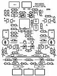
R23 and R24 for Spooky
Hi Jan,
this is what OS wrote http://www.diyaudio.com/forums/solid-state/248105-slewmaster-cfa-vs-vfa-rumble-920.html#post4687811
For example - spookyamp
- 7.4ma VAS (2.1 led's + 5.3ma output)
- 14ma through the 3.9K zener resistors (7ma zener + 3 LTP + 3 op-amp)
I'm using about 22ma per rail total.
Total can change with different VAS/differential current settings.
If you just count the zener I , you might think a smaller resistor will work.
The resistor current actually is the zener,CCS, and op-amp (I) .
In the real world , even a 1W device gets quite warm.
Another "trick" is to just use the highest value R you can to get 12V at
the shunt.
PS - to cover almost anything , a 2W 3.9K will cover 45-75V.
A 1W will do if you calculate the R for the rail voltage.
A 1W even at 3.9K will get hot , but not burn. Mount it above the board.
Guy's is this correct ? What puzzles me is that 0V input is directly connected to the same node where R2/C2 is connected. Will this not shunt the signal from R33 ? If you look at Spooky V1.3 you will see what I mean. Look where the 0 volt input connects at ground. That's why I say 0V input has to change as well.
Jan, you need to cut R33 from G2 power ground point and then connect it to R2 as you did with your red line. So, just add a "cut" between the bottom of your red line and G2. Exactly as V1.3 shows.
If you look at what I wrote in post #2070:
"You just need to cut R33 from the power ground and connect it to R2." 😉
post2072Guy's is this correct ? What puzzles me is that 0V input is directly connected to the same node where R2/C2 is connected. Will this not shunt the signal from R33 ? If you look at Spooky V1.3 you will see what I mean. Look where the 0 volt input connects at ground. That's why I say 0V input has to change as well.
V1.3 is wrong as well.
Vin is connected to power ground !
Vin is a signal, not a power connection.
This error was discussed some months ago.
At that time many were arguing that all the different schematics were correct.
Eventually it was agreed that the NFB must connect to the signal input.
Why are the incorrect schematics still showing in the various Threads?
Some one with authority should have identified all the incorrect sch and arranged for ALL errors to be removed.
Then OST could at his leisure come back and replace with the corrected versions.
This Forum should not contain incorrect sch. Remove sch that are proved to be incorrect. That should be written into the rules !
Last edited:

No.
the TWO wires from Vin must connect to the INPUT circuit.
Connect the two red additions.
I think C11 is connected incorrectly.
It shows the servo being connected to power ground. I think (not sure) this is also wrong.
I wonder if this is why there were reports that some of the servo circuits were not working correctly.
- Home
- Amplifiers
- Solid State
- SlewMaster Builds