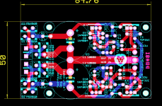
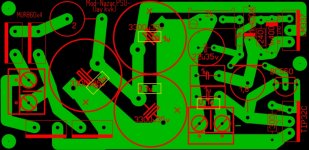
Attached is the dual PS layout that Prasi sent me some time ago, but I am not sure this is the final or not. Assuming it is, and it is the top view. Then take a look at T1, the BC560C's pin 1 (collector) is connected to T3's pin 1 (base). It should be pin 3 (emitter) of the BC560C connected to T3's pin 1. In other words, the orientation of T1 is reversed. The -ve rail probably has the same issue as well.
Take the T1 out and put a new one in and reverse orientation as in the PCB to see it works.
Good luck!!
Take the T1 out and put a new one in and reverse orientation as in the PCB to see it works.
Good luck!!
Attachments
If you have to change anything from the original values, then it doesn't work. It just happened to "look like" working.Why does mine work? Or maybe it doesn't really as had to change R to 100.
The easiest way to look at this is, the 240R (call it TOP) and the 1K+VR3 (call it BOTTOM) form a ratio to adjust the output voltage. The larger the BOTTOM, the more voltage you get. However, if the BOTTOM is somehow logically in parallel to a low resistance., then the ratio of the TOP can be >>> the BOTTOM. Hence, changing the VR has no effect. When you lower the TOP, the ratio might become TOP > BOTTOM, and to a point, the VR started having some effect. The fact was, the shunt simply didn't work.
Since you have the board, it is easy to check with a DMM to see whether pin3 of T1 is connected to pin 1 of T2. Pin 3 of the BC560C is the right pin when the flat side facing you and the legs pointing down. I just did a quick check to the LM317 rail boards that I ordered in early Dec. It indeed had the same issue - the orientation of the BC560C on the board is reversed.
My bad, the BC560 orientation is actually correct. I compared it to my working hacked up single rail version. I will populate one of the boards and give it some measurements.
Hi Eric, I did use 330R instead of 300R for R11/12, as didnt have it. I also had some D45H11/D44H11.Hi Prasi,
I'll wait before building mine. Have you used the exact value as per the schematics. Hopefully this can be resolved.
Eric
I am sure it will work with TIP's / the transistors XRK is using.
Prasi
Yes Fred, that is the final version, I have only added LED across the o/p for indication.Attached is the dual PS layout that Prasi sent me some time ago, but I am not sure this is the final or not. Assuming it is, and it is the top view. Then take a look at T1, the BC560C's pin 1 (collector) is connected to T3's pin 1 (base). It should be pin 3 (emitter) of the BC560C connected to T3's pin 1. In other words, the orientation of T1 is reversed. The -ve rail probably has the same issue as well.
Take the T1 out and put a new one in and reverse orientation as in the PCB to see it works.
Good luck!!
As pointed by later, T1's orientation is correct as per the Nazar's article or Stixx's schematic..
I have a doubt on my LM's as they were sourced locally🙄.
reg
Prasi
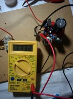
I just populated one single rail LM317 board. It fired up with no instance. I used a 12VAC transformer, and the lowest voltage matched Andrew's voltage in post #448 - one Vbe. So, it is working as advertised. I can't imagine the dual board is that much of a difference.
FWIW, I am NOT using the tip, I have a D44H11.
In general, the cap after the LM317 should never be a low ESR cap. X, looks like you have a stack film cap at that position, which is a big no no. You should replace it with an electrolytic, a 2.2uF or a 4.7uF will do just fine.
For trouble shooting purpose, I will strip the shunt portion, test, and measure the output. Without the shunt part, it should be just a plain LM317/LM337 reg board. If it measures up, add the shunt one rail at a time. Basically, just to find the point that the circuit breaks.
LOL, can't imagine who can make money by faking LM's 😀Yes Fred, that is the final version, I have only added LED across the o/p for indication.
As pointed by later, T1's orientation is correct as per the Nazar's article or Stixx's schematic..
I have a doubt on my LM's as they were sourced locally🙄.
reg
Prasi
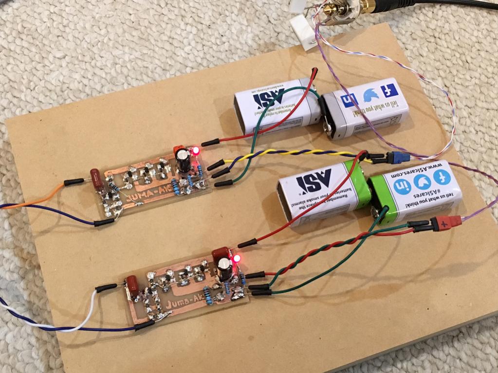
I also used an unknown LM317 when I did the quick test - the brand of the LM317 was SD😕 Anyhow, here are 2 pictures of the board and measurements. It is obvious that I was able to adjust the voltage up and down as it should.
Whatever is the cause of the symptom, it is likely to be something simple.
Attachments

do we need to load the o/p with a resistor, like your picture shows when doing adjustments?LOL, can't imagine who can make money by faking LM's 😀
I also used an unknown LM317 when I did the quick test - the brand of the LM317 was SD😕 Anyhow, here are 2 pictures of the board and measurements. It is obvious that I was able to adjust the voltage up and down as it should.
Whatever is the cause of the symptom, it is likely to be something simple.
In general, the cap after the LM317 should never be a low ESR cap. X, looks like you have a stack film cap at that position, which is a big no no. You should replace it with an electrolytic, a 2.2uF or a 4.7uF will do just fine.
.
Wow, I too have kemet polyester film cap in that position. I will replace with a 2.2 or a 10 uf cap and retest today evening.
I don't think so even though I always attach a load whenever I fire up the reg.do we need to load the o/p with a resistor, like your picture shows when doing adjustments?
In reality, the 240R connected to the adjust pin is pulling 5 ma already. Perhaps check the voltage along the junctions of the 240R <-> 1K <-> VR3 while varying VR3. If it doesn't change, then it can be a broken VR3.
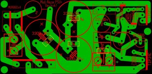
here is the final layout used for production except d10 orientation. i cant find any mistakes except, d10 which in this layout is corrected.
if anyone can make a suggestion, most welcome.
i have changed 3 pairs of LM's till now, without any benefit in adjustment. i changed the caps too (c5/c6=10u electro)), no change. in this process, i managed to damage many pads. i dont think pcb will take any more abuse.
i will order some more if any one willing to test and offer correction.
i have also ordered lm's from RS components. such hopeless experiences make me hate local/ (mostly Chinese) components
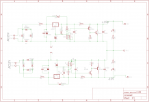
i am of the mind to drop the shunt components and use it as a lm reg which would still be more than suitable for juma ha. here is the asc file and also the schematic (corrected for d10) for dual rail.
if anyone can make a suggestion, most welcome.
i have changed 3 pairs of LM's till now, without any benefit in adjustment. i changed the caps too (c5/c6=10u electro)), no change. in this process, i managed to damage many pads. i dont think pcb will take any more abuse.
i will order some more if any one willing to test and offer correction.
i have also ordered lm's from RS components. such hopeless experiences make me hate local/ (mostly Chinese) components
i am of the mind to drop the shunt components and use it as a lm reg which would still be more than suitable for juma ha. here is the asc file and also the schematic (corrected for d10) for dual rail.
Attachments

What's strange is that the adjustment works on my board with change in D10 orientation and 100R vs 240R for R3 and R6. I am using cheap LM's from aliexpress and seems to work. I can get 13v to 18v adjustment range. The lower voltage gets the BJT really hot. Oh, I am not using TIPs there but more audio type BJT - SA1930 and SC5171 (labeled Toshiba). So I suspect that you have bad LM's. Try wiring an LM outside deadbug to see if it works. Just needs pot and 2 resistors I think. Can do it straight off legs to check to see if they work. Are your TIP's known to be working?
Have you tried bypassing all the add on circuitry and running the regulators as the datasheet suggests for troubleshooting? Jumper R1 and R9 in the positive side and remove T1 and it should run. C1 is pretty huge for a small transformer to try to charge.
I had a very silly mistake on board,  , intead of 1k, i had 6k8 res , can you believe that?
after changing the resistor, i was able to adjust positive voltage to 15V.
wait, tragedy doesn't end here, the pot on negative rail was faulty, so while changing the 1k res and the pot, i managed to damage the pcb, so negative rail doesn't adjust...
looks like i need to order more pcb...
I hope Thimios gets his set quickly and is able to test quickly.
so the lesson to builders would be measure twice and solder once...
reg
Prasi
, intead of 1k, i had 6k8 res , can you believe that?after changing the resistor, i was able to adjust positive voltage to 15V.
wait, tragedy doesn't end here, the pot on negative rail was faulty, so while changing the 1k res and the pot, i managed to damage the pcb, so negative rail doesn't adjust...
looks like i need to order more pcb...
I hope Thimios gets his set quickly and is able to test quickly.
so the lesson to builders would be measure twice and solder once...
reg
Prasi
Last edited:
I had a very silly mistake on board,
after changing the resistor, i was able to adjust positive voltage to 15V.
wait, tragedy doesn't end here, the pot on negative rail was faulty, so while changing the 1k res and the pot, i managed to damage the pcb, so negative rail doesn't adjust...
looks like i need to order more pcb...
I hope Thimios gets his set quickly and is able to test quickly.
so the lesson to builders would be measure twice and solder once...
reg
Prasi
I mess up resistors all the time. Usually it's off by 100x. Like 3k3 vs 330k etc.
we should probably always measure resistors prior to inserting. But we don't.
Here is my version of a compact single-sided PCB PSU for "laser printer's technology"
Attachments
Last edited:
Here is my version of a compact single-sided PCB PSU for "laser printer's technology"
For simple layouts with large features, I often just use a Sharpie permanent ink marker on copper as the resistor for etching. See my SE Class A headamp made this way:
Last edited:
Did you get local pots or did you order from rs or the likes?I had a very silly mistake on board,
after changing the resistor, i was able to adjust positive voltage to 15V.
wait, tragedy doesn't end here, the pot on negative rail was faulty, so while changing the 1k res and the pot, i managed to damage the pcb, so negative rail doesn't adjust...
looks like i need to order more pcb...
I hope Thimios gets his set quickly and is able to test quickly.
so the lesson to builders would be measure twice and solder once...
reg
Prasi
Sent from my A0001 using Tapatalk
- Home
- Amplifiers
- Pass Labs
- Juma's Head Amp