Good morning Kartino, it is possible to remove the pre-balanced and leave unbalanced and use that your pre "Litina"
Kees,
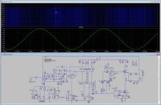
Nice, but I don't understand some things. Why do you call the 1st one digital? If timing was discrete only then it was digital. Why switching freq changes asymmetrically, and why do you accept it? What "HD" stands for? And please adjust window size of FFT to whole periods to avoid spectral leakage!
About the second sim:
Hysteretic ucd is an oximoron. UcD is free of hysteresis (check in patent!). And doesn't use pre-filter feedback at all. And why to mention 2nd harmonic in a basically symmetric circuit when there is a 30 dB bigger 3rd harmonic?
Generally: to design a practically useful schematic there are further requirements above switching freq and distortion:
- Low idle loss and low distortion at small signal (these are contradictional requirements!)
- Low loss at nominal power.
- Low output offset voltage with unmatched components
- Acceptable temperature dependency of the above mentioned parameters (may be checked with temp parameter stepping)
- Low sensitivity to parasitic effects
- Good overdrive behaviour
- Safe turn on and off behaviour
- Stable and safe operation without load
- Fast overcurrent protection
- Overvoltage protection
- Stable and safe operation without input source
- ...
Hehehe yes I do make a mistake, the term digital is misplaced but a lot do call it such way because of the switching behavior. The schematics are just from the internet and what concerns LTspice still after use a year I have still not yet find all the possibillities, I am happy when learn more with tips like you did thanks. I was plan to hide the 800 Khz switch frequentie from FFT to see things more clearly, but as I say class D is new for me, and I am quite green behind the ears with that.
So have in mind that I have no experience whatsoever with class D amplifiers but I do like the technology behind it, for as these amps concerns I have openen a own thread so I do not hijjack this one.
The schematics are just examples the protections can be easely implemented by supply line sensor who give a off voltage and a delay.
A open output of a switching amp is always a troublesome problem because the low pass sees a high impedance the whole thing go in stress it is mention also over the internet, design a class D is not that simple, but making a pwm version with own clock do have a lot less impact on open output.
Al the questions you did ask I do now that is something who also need considered afcouse, what I did is just something from internet and recalc for what I did to get what I want, the power comparator in picture has protections in it however I have not use it in sim, it is a excistent schematic who has a 105 nS delay.
For offset demands, I have a circlotron on hand, and these allfet liniair amp needs also matched components, it is always the best way to do that.
regards
Attachments
Last edited:
Hi Pafi can you explane me how to set FFT in ltspice the best way? like
you say here
And please adjust window size of FFT to whole periods to avoid spectral leakage!
Did you mean to set lower so i see not the carrier?.
thanks, and sorry I did not answer all the questions, I am new in class D, but interesting thead here.
I have info and power comparator from here,. why a hysteric window is not used? self oscllating amps do when
be hard driven lower the oscillating frequenty, in the paper is also written that a fase shift osilating amp has lower
distortion and less drop of carrier.
http://www.hobbielektronika.hu/forum/getfile.php?id=253790
regards
Last edited:
Good morning Kartino, it is possible to remove the pre-balanced and leave unbalanced and use that your pre "Litina"
As Pafi said, clarity will be less
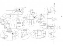
The schematics are just from the internet
The schematic is very old.
How to drive the mosfet is not good enough for a good class D amp.
I give you all bonus, UcD200, with PCB this time.
Sorry for PCB some pad and track still touch each other or very narrow gap. You need to check before etching. PDF printing problem
Transistor replace
Good morning Kartino, it is possible to remove the pre-balanced and leave unbalanced and use that your pre "Litina", And the transistor can be replaced by 2n5401=mpsa92 , 2n5551= mpsa42
Let show my circuit.
It is:
- Low idle loss and low distortion at small signal (these are contradictional requirements!)
- Low loss at nominal power.
- Low output offset voltage with unmatched components
- Acceptable temperature dependency of the above mentioned parameters (may be checked with temp parameter stepping)
- Low sensitivity to parasitic effects
- Good overdrive behaviour
- Safe turn on and off behaviour
- Stable and safe operation without load
- Fast overcurrent protection
- Stable and safe operation without input source
Sorry no overvoltage protection required for me, as my experience, pumping effect is less than 10% nominal.
Bonus: DC Protect and Front Signalling.
Sorry no PCB for share.
Good morning Kartino, it is possible to remove the pre-balanced and leave unbalanced and use that your pre "Litina", And the transistor can be replaced by 2n5401=mpsa92 , 2n5551= mpsa42
I give you all bonus, UcD200, with PCB this time.
Hi
Thanks for the schematic, it is the phillips based class D with a good exception, a cascode in the comparator, as for old schematics, class D is stalled on some level, there a many efforts to make it more perfect, I have respect for you guys to experiment on it, class.
For me the examples are just for info, for a complete one from own hands, I need extensive learning to do, and most is not to make in discrete way because of pcb issieus.
The schematic is very old.
How to drive the mosfet is not good enough for a good class D amp.
What schematic do you refere from? last post?. maybe use of gate driver chips are
a better way to do but last schematic has delay of 120 nS, who is quite fast
if schematic is right but can sim that easely.
Reason fror them was save extra supply for the low voltage chips, but maybe it
is better with separate supply for drivers because in smps world ( I am have made a
weld inverter 140 amps) she use always separated supplys to make it imune from out
put pulses, making a good switch amplifier is not the simple because of this.
regards
Last edited:
Hi Pafi can you explane me how to set FFT in ltspice the best way?
I posted this to your thread.
I have info and power comparator from here,. why a hysteric window is not used? self oscllating amps do when
be hard driven lower the oscillating frequenty, in the paper is also written that a fase shift osilating amp has lower
distortion and less drop of carrier.
You've answered your question (if I understand it correctly).
The article is very good (thanks!), but in the schematic I think there is a mistake, in low side driver value of R22 and R24 must be swapped. This could explain why switching freq varies asymmetrically.
Let show my circuit.
It is:
- Low idle loss and low distortion at small signal (these are contradictional requirements!)
- Low loss at nominal power.
- Low output offset voltage with unmatched components
- Acceptable temperature dependency of the above mentioned parameters (may be checked with temp parameter stepping)
- Low sensitivity to parasitic effects
- Good overdrive behaviour
- Safe turn on and off behaviour
- Stable and safe operation without load
- Fast overcurrent protection
- Stable and safe operation without input source
Sorry no overvoltage protection required for me, as my experience, pumping effect is less than 10% nominal.
Bonus: DC Protect and Front Signalling.
Sorry no PCB for share.
Kartino,
This one is better, however there are some embarrassing small mistakes. And I don't believe you really checked it for all the features you copied from me but forgot to indicate quotation.
Regarding overvoltage:
Try to short output through a long, thick wire, without input signal, and measure supply voltages (unless the amp is already exploded)!
As Pafi said, clarity will be less
I never said this. I advised unbalanced drive but on the other input, the noninverting one.
I don't have any complete amp schematic to share since I designed all of my ClassD amps directly on PCB, with some basic theoretical simulation. Except for the first one (15 years ago, on paper) and my current design. But I posted here many details, and a photo of a complete (LLC PSU+UcD 800 W) amp also that has been reverse engineered immediately by an experienced member. I don't want to heal the world.
all the features you copied from me but forgot to indicate quotation.
Regarding overvoltage:
Try to short output through a long, thick wire, without input signal, and measure supply voltages (unless the amp is already exploded)!
I never said this. I advised unbalanced drive but on the other input, the noninverting one.
Can you clarify what are copied from you?
I mean by cutting the op amp stage it can affect to feedback as one of input is grounded
everyting salvage
https://www.youtube.com/watch?v=OyQ0Cof_QbU
OK then
So everybody are talking about small amp while I.am talking big big amp. That is why everybody talking clarity since from simulation.
It is difference approach when you make big amp. Dont bother.clarity at beginning but how the amp.can survive.or.become ash. Then start improve clarity. Yes it is take time.
I don't have any complete amp schematic to share since I designed all of my ClassD amps directly on PCB, with some basic theoretical simulation. Except for the first one (15 years ago, on paper) and my current design. But I posted here many details, and a photo of a complete (LLC PSU+UcD 800 W) amp also that has been reverse engineered immediately by an experienced member. I don't want to heal the world.
I take note on this 😀
Understand, and the last sentence as well
What schematic do you refere from? last post?. maybe use of gate driver chips are
a better way to do but last schematic has delay of 120 nS, who is quite fast
if schematic is right but can sim that easely.
Reason fror them was save extra supply for the low voltage chips, but maybe it
is better with separate supply for drivers because in smps world ( I am have made a
weld inverter 140 amps) she use always separated supplys to make it imune from out
put pulses, making a good switch amplifier is not the simple because of this.
regards
All schematic with passive charging gate cannot be fast enough for clasd D. 100ns delay is not good for a small amp.
Can you clarify what are copied from you?
The feature list. (What was more than half of your post.)
I mean by cutting the op amp stage it can affect to feedback as one of input is grounded
I can't see this means anything. And I ask you not to refer to me when writing things like this. Balanced and noninverting inputs behave very similarly. Unbuffered inverting input is totally different.
All schematic with passive charging gate cannot be fast enough for clasd D. 100ns delay is not good for a small amp.
I agree, it's not good. It's excellent. 🙂
OK then
So everybody are talking about small amp while I.am talking big big amp. That is why everybody talking clarity since from simulation.
It is difference approach when you make big amp. Dont bother.clarity at beginning but how the amp.can survive.or.become ash. Then start improve clarity. Yes it is take time.
No difference. All principles are the same for any size. OK, above 2 kW other topologies and methods worth to be considered. I built some with 150V and 30A continuous output and 200 kHz switching freq about 8 years ago, and they were almost the same quality as the smaller ones. Instead of 0.1 % it has 0.3 % THD, but not 3 %! Others make 50 kW in one rack unit and much better quality. That is a big amp. We are nothing.
- Home
- Amplifiers
- Class D
- UCD 25 watts to 1200 watts using 2 mosfets