You really are obsessed with single PCB's. You could make one for this juma HA and mod nazar psu show it to the forum😉. i will buy one from you...Re-using left over parts/PSU's is the main reason why separate boards exist 😀 It is not better, it is only convenient. Only to save a few $ on capacitors and some semis....Without noticing working like this is running in circles.
So with final choice for one board designs leftover stuff will find its way to other leftover stuff. Better new single board designs with short signal paths and no wiring will be born. All over quality will be better. Devices can be more compact, reproducibility is more consistent. Less questions asked by unsure builders. No vague grounding issues. Devices will be built and ready for use. Discussion will be on parts and not comparing apples with pears. Parts can be bought in quantities and in possible GB or kit form with PCB. No leftover PSU's will be created so better ROI. Audiophiles will be more happy. Designer will have less support questions to answer. Problem solved 🙂
I suppose somebody has been burned by excessive user complaint calls about integrated system hum, noise, etc. 🙂
I agree, you can control a lot more of the process with a single board, but it also understood that this is DIYA and we are here to learn as well. I don't come here expecting someone to hand me a perfectly working *system* and I have no right to make complaints if it doesn't work perfectly either.
I agree, you can control a lot more of the process with a single board, but it also understood that this is DIYA and we are here to learn as well. I don't come here expecting someone to hand me a perfectly working *system* and I have no right to make complaints if it doesn't work perfectly either.
You really are obsessed with single PCB's. You could make one for this juma HA and mod nazar psu show it to the forum😉. i will buy one from you...
Ha ha ;-) I get no real counter reasons in return so I guess it depends who is the obsessed 🙂
@xrk971: learning is also designing pcb's !
Last edited:
...chime in with some tips ...
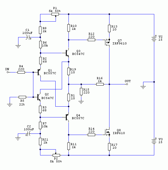
I don't know the exact schematic of your complete build (headamp, power supply and "cross-feed-volume-control") but here are some guidelines:
- this headamp should be fed from the signal source with Zout of 1k or less (buffered pot would be fine). To accommodate for signal sources with higher Zout, R5 should be changed to 100k but it might lead to DC offset at the input (solvable with 1uF input coupling capacitor inserted between R4 and the input)
- the circuit is designed for +/- 15 V, regulated power supply which is capable of reliably delivering few hundreds mA of current without hickups - 7{8,9}15 regs will do for a start
- the current through input BJT pair should be about 1mA (can be measured as voltage drop across R2 or R3. This is set by turning the P1/P2 (raising the resistance lowers the current)
- the current through second BJT pair (Q3/Q4) should be about 4-5mA (it's dependent on current through Q1/Q2) and is measured as voltage drop across R10 or R11 - this voltage drop determines the Vgs and Id (bias current) of output MOSFETs.
Bias current should be adjusted with two Voltmeters (one connected from output to ground to measure 0 V DC offset and the other across R13 or R17 - 1 Volt represents the Id of 100mA). Adjustment should be done in small steps, bu turning both pots alternatively.
- thermal stability is achieved by Source degeneration (R13/R17) and adequate heatsinking.
- don't change the gain settings (R16/R15) - it's not just the volume that you affect by doing it but the stability of the circuit too
- Using chinese/fake parts will require some changes so if the bias is too high at maximum resistance of pots the value of R8/R21 should be raised (say, 4k7).
- Try to stay away from parts made/remarked/faked in "chinese wilderness". They save you a penny or two but you pay more for it by debugging the troubles they cause...
Hi Juma,
Thank you for the guidance. This is really helpful.
The circuit follows your schematic with a few modifications, which I now realize is the source of the low volume. In post 3, AndrewT suggested changing the feedback resistance to lower the gain as 15dB would be too high for his headphones. He did caveat that with checking for stability margins. So it is shown on silkscreen as 390R for R16 (actual value on mine is 420R). I will go back to your specified 1k. I am indeed using 7815 and 7915 regulators. Will check the currents through first and second stages and set pots at 50% wiper. I am going to bypass the input cross feed filter now. Let's see if that improves things.
Here is your schematics:
Here is the modified schematic which includes input RF filter and 10R ground lift and protection diodes on input ground.
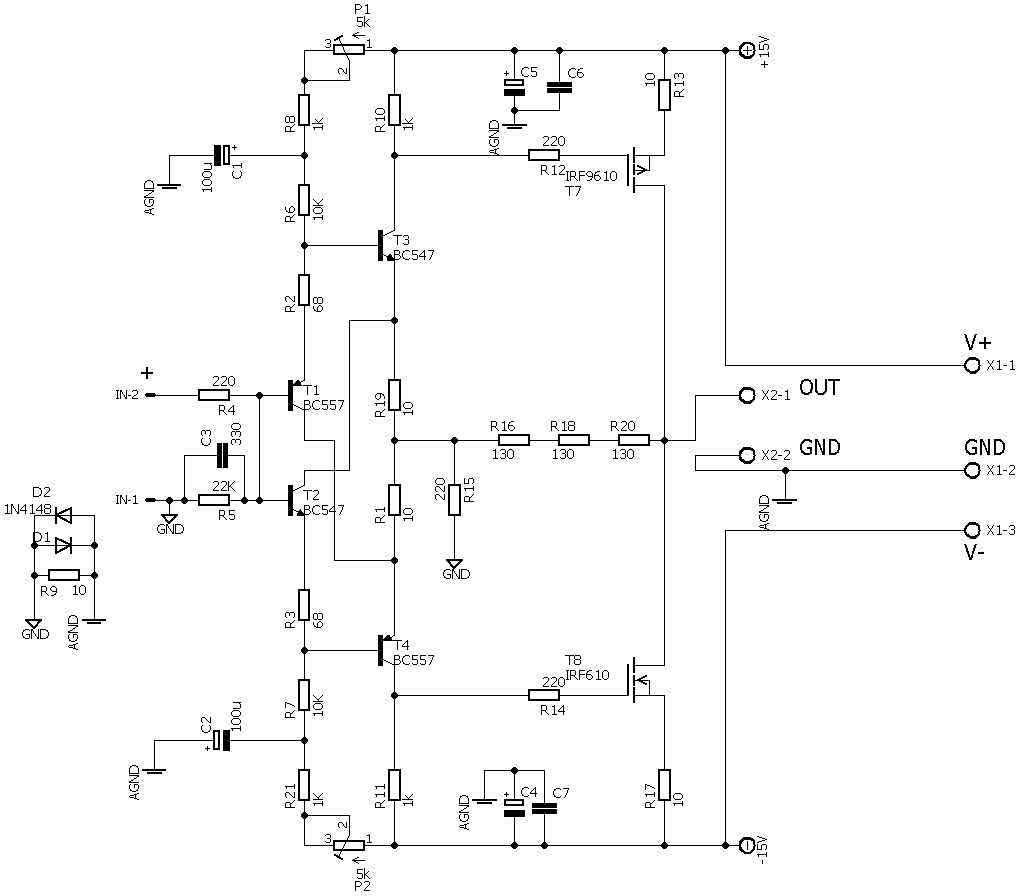
I am using real Vishay IRF's from Digikey so can be certain of their provenance. Although resistors and pots are Chinese but values check out well.
Thank you for the guidance. This is really helpful.
The circuit follows your schematic with a few modifications, which I now realize is the source of the low volume. In post 3, AndrewT suggested changing the feedback resistance to lower the gain as 15dB would be too high for his headphones. He did caveat that with checking for stability margins. So it is shown on silkscreen as 390R for R16 (actual value on mine is 420R). I will go back to your specified 1k. I am indeed using 7815 and 7915 regulators. Will check the currents through first and second stages and set pots at 50% wiper. I am going to bypass the input cross feed filter now. Let's see if that improves things.
Here is your schematics:
Here is the modified schematic which includes input RF filter and 10R ground lift and protection diodes on input ground.
I am using real Vishay IRF's from Digikey so can be certain of their provenance. Although resistors and pots are Chinese but values check out well.
I changed the feedback resistors to all = 330R for R16 single value equivalent of 990R now. The gain is now loud enough even going through the cross feedbfikter with R5 set at 100k.
However, to get balanced 0vdc out I am only able to get as low as 200ma bias. The voltage across R2 is 74mV or 1.09mA. The voltage across R3 is 59mV or 0.87mA. That's a big disparity to get 0vdc at the output. The Hfe for both Q1/2 is 470. I have BC547/557c's and they are also in the same Hfe range so I don't think it's because I am using BC550/560c's that's causing the issue. Voltage across R10 is 6.59v or 6.59mA. Voltage across R11 is 6.66v or 6.66mA. Maybe Q3/Q4 Hfe need to be matched better? Gate voltages on Q7/Q8 are 8.41v and 8.32v, respectively.
However, to get balanced 0vdc out I am only able to get as low as 200ma bias. The voltage across R2 is 74mV or 1.09mA. The voltage across R3 is 59mV or 0.87mA. That's a big disparity to get 0vdc at the output. The Hfe for both Q1/2 is 470. I have BC547/557c's and they are also in the same Hfe range so I don't think it's because I am using BC550/560c's that's causing the issue. Voltage across R10 is 6.59v or 6.59mA. Voltage across R11 is 6.66v or 6.66mA. Maybe Q3/Q4 Hfe need to be matched better? Gate voltages on Q7/Q8 are 8.41v and 8.32v, respectively.
Last edited:
That's too much. Change R2 = R3 = 33R instead of 68 R. The current through input pair is OK.... R11 is 6.66v or 6.66mA ...
That's not a meaningful measurement. Measure voltage between the gate (pin 1) and the source (pin 3) of the MOSFETs. That's Vgs, the controlling voltage that sets the current through MOSFET.Gate voltages on Q7/Q8 are 8.41v and 8.32v, respectively.
Anyway, if you have 6.66V across R10/R11 and Id=200mA it means that your MOSFETs operate at Vgs = 4.66 V and yes, it's a hefty bias for a push-pull headamp. However, I find that HEXFETs tend to sound better with more bias current so I'd rather support them with biger heatsink (it's only 3W per MOSFET), but you can test them at different bias levels and find what you like the best...
On the second channel I replaced the BC550/560 with BC547/557c's and still getting the same 210mA minimum bias. If current on input pair is good why am I changing R2/R3 to half the value? Would it not be R10/11 that needs be 2k vs 1k?
Listening in stereo sounds very nice. I am getting some noise pickup in the volume pot and headphone jack. When I turn volume all the way up it goes away and when I touch the headphone shell the noise is reduced. This did not happen with the F5HA with JFETs input.
It may be the 100k input resistor is allowing the amp to pick up noise? On F5HA input resistor was also 100k.
Listening impressions so far is that the sound is very balanced. Great bass and very clear highs with good articulation. Excellent vocals and smooth mids.
The difference with JFET F5HA is that the volume pot makes noise when I turn it now and there is some noise pickup in the pot/cross feed apparatus. Have not had chance to go straight from source yet.
Anyhow I have to stop here for today - as it is Thanksgiving so may be a few days before revisiting.
Last edited:
In order to make the current through second pair lower without changing the current through input pair.... why am I changing R2/R3 to half the value?...
That would double the Vgs of the MOSFET and skyrocket the bias current. And lowering the value of R10/11 would lower the OLG of the headamp and change its character....Would it not be R10/11 that needs be 2k vs 1k? ...
Depending on how you wire it, "free air" construction tends to pick up noise, so proper grounding and the box are needed to really evaluate the headamp....It may be the 100k input resistor is allowing the amp to pick up noise? ...
This indicates small DC voltage at the input and that needs either lower value of R5 or the coupling cap - I mentioned that already in post # 224.... the volume pot makes noise when I turn it ...
Patrick's headamp has JFETs at the input and they normally work with Ig=0 so there's no DC offset at the input with them. BJTs work with Ib and if we use pair unmatched by Vbe/hfe there will be some DC at the input (and how much of it will depend on matching and the value of R5).
Last edited:
Hi Juma,
You said a buffer after the volume pot is required, can you suggest a super simple op-amp based buffer, if you have it already. I want to make a tiny volume control PCB with op amp buffer so that it can be mounted on front panel/ or as a daughter PCB on your HA (stereo version).
something similar to the one here. http://www.diyaudio.com/forums/solid-state/70276-simple-volume-buffer.html#post797211. unfortunately the designer there no longer could be contacted.
reg
Prasi
Hi Juma,
You said a buffer after the volume pot is required,.../QUOTE]
10k pot will have Zout=2k5 in worst case and that;s tolerable - the buffer is needed if you use the source xrk mentioned (Zout=5k5).
Any buffer in line of B1 is OK - it can be made with BF862, J310 and many more - 2sk170 is not mandatory JFET for such a circuit
xrk,
I get the impression you don't understand the DC, or quiescent, operation.
Do you want/need a layman's explanation?
I get the impression you don't understand the DC, or quiescent, operation.
Do you want/need a layman's explanation?
Last edited:
Hi Juma,
You said a buffer after the volume pot is required,.../QUOTE]
10k pot will have Zout=2k5 in worst case and that;s tolerable - the buffer is needed if you use the source xrk mentioned (Zout=5k5).
Any buffer in line of B1 is OK - it can be made with BF862, J310 and many more - 2sk170 is not mandatory JFET for such a circuit
I have J310 and SK170 so B1 approach is good as it is simple and Transparent.
So the advantage of the F5HA is that it has FET inputs which allows passive volume to be used as if it had a buffer. So simpler circuit by 4 actives now if a B1buffer were to be added. Although the character of this current feedback amp is different than F5.
Last edited:
xrk,
I get the impression you don't understand the DC, or quiescent, operation.
Do you want/need a layman's explanation?
Sure. After thinking about it more I see that reducing R2/R3 to 33R will give less current to second stage and thus lower its output current and thus less drive voltage to the MOSFETs.
using your sch:
two assumptions to start off.
a.) the input offset voltage is zero, i.e. the base currents of T1 and T2 are exactly equal.
b.) the output voltage is zero, i.e. the voltage at the junction of R1 and R19 is exactly zero.
Starting from the base of T1 @ 0.000Vdc your path takes you up to the emitter of T1. It sits at ~0.6Vdc
Carry on up through R2. The current through R2 creates a Vdrop = Vr2 for 1mA of emitter current the voltage at the top of R2 is now at 0.600Vdc + 0.068Vdc = 0.668Vdc
Now come back down through the BE junction of T3. This makes the voltage at T3 emitter roughly 0.06Vdc .
The volts drop through R19 is Ir19 * R19
We know that the voltage at the bottom of R19 is zero volts.
Turning that into an equation we get
VbeT1 + Ir2*R2 = VbeT3 + Ir19*R19 or VbeT1 + Vr2 = VbeT3 + Vr19
Rearrange this to find Ir19 and we get:
Ir19*R19 = VbeT1 + Vr2 - VbeT3
We know that the two Vbe do not change much after they have warmed up. So measure these after a short warm up.
Measure Vr2
Put those values into that last equation.
We get Ir10*R19 = ~600mV +68mV - 620mV = 48mV
Therefore Ir19 ~48mV/R19 ~ 4.8mA
The current through R2 determines the current through R19.
Analyse the lower half and you will find that the current through R1 is determined by the current through R3.
Due to the symmetry in the upper and lower halves these currents are equal.
If you want to change the current in R1 & R19 you change the Vdrop of R2 and R3
These currents have ignored the hFE of the 4 input transistors. Since the hFE of these is >>200 there is very little error in ignoring the effect of the base currents.
Move on to the last stage.
We have the predetermined equal currents in R1 and R19
Those currents have to pass through R10 and R11, giving Vdrop = R10*Ir19 = R11*Ir1
Here is the last assumption:
c.) the current through R13 exactly equals the current through R17. This is the only necessary condition to allow the output offset to be zero (assumption b.)
Now let's set up the equation for the output device.
Vdrop of R10 = Ir10*R10 = VgsT7 + Ir13*R13
We re-arrange this to Get Ir13*R13 on the left
Ir13*R13 = Ir10*R10 - VgsT7
Therefore Ir13 = {Ir10*R10 - VgsT7} / R13
and you have for the lower half:
Ir17 = {Ir11*R11 - VgsT8} / R17
Both the output device currents depend on the current passing through the middle stage. And the current through the middle stage depends on the currents passing through the first stage.
You can change the current in any stage by changing the resistor values.
Finally,
we know from experience that Vgs of an Nchannel mosFET does not equal the Vgs of a Pchannel mosFET. That throws everything out of equality.
Well not quite. There are two adjustable Current Sources feeding the currents into that first stage.
WE can make small adjustments to the first stage CS to correct for errors in the output stage currents. Remember we must make the output stage currents exactly equal to get zero output offset.
If there is a big error in the symmetry of the upper and lower currents, then stop altering the CS adjuster. Instead reset the CS adjusters to pass identical currents.
Set the resistor values in the input and middle stages to get the recommended currents.
Then remove some of the asymmetry in the output stage by adjusting either R10 or R11. This is what the pots do in an F5. There they set up the symmetry in the input stage and adjust the output stage by changing the Vgs values.
Last edited:
If one takes a poll on Andrew's best post, this one will be my numbah 1. Thanks Andrew!
As AKSA said somewhere, DC analysis of a ckt is the most important aspect.
reg
Prasi
As AKSA said somewhere, DC analysis of a ckt is the most important aspect.
reg
Prasi
Last edited:
I can't do AC analysis and that means I can't design amplifiers.
But I can do simple arithmetic and apply simple logic to what I see.
DC analysis seems to fit within my abilities.
So that is what I try to spread. It's not difficult.
ps.
does your poll imply that some of my posts are less good?
But I can do simple arithmetic and apply simple logic to what I see.
DC analysis seems to fit within my abilities.
So that is what I try to spread. It's not difficult.
ps.
does your poll imply that some of my posts are less good?
Hi Andrew,You have shown the path... that one can follow.I can't do AC analysis and that means I can't design amplifiers.
But I can do simple arithmetic and apply simple logic to what I see.
DC analysis seems to fit within my abilities.
So that is what I try to spread. It's not difficult.
🙂🙂... Your posts are always good, this is the best one... is all I meant... if i see your older posts, you used to greet with a 'Hi' in some of your posts... Now its missing... although its more practical to come to the point rightaway😉...ps.
does your poll imply that some of my posts are less good?
- Home
- Amplifiers
- Pass Labs
- Juma's Head Amp