It's early still here in the USA, but many gurus are in Europe or India so I expect we will see something soon. Patience is a must when asking for handouts 🙂
But if you are in real hurry, just P2P it like I did.
But if you are in real hurry, just P2P it like I did.
Trust you noticed R15 1.5K also sees the full ac output voltage across it due to bootstrapping.
Trust you noticed R15 1.5K also sees the full ac output voltage across it due to bootstrapping.
Where is R15? There is a 1.5R resistor that appears to be a snubber with 1uF. I don't see any 1.5k resistor ?
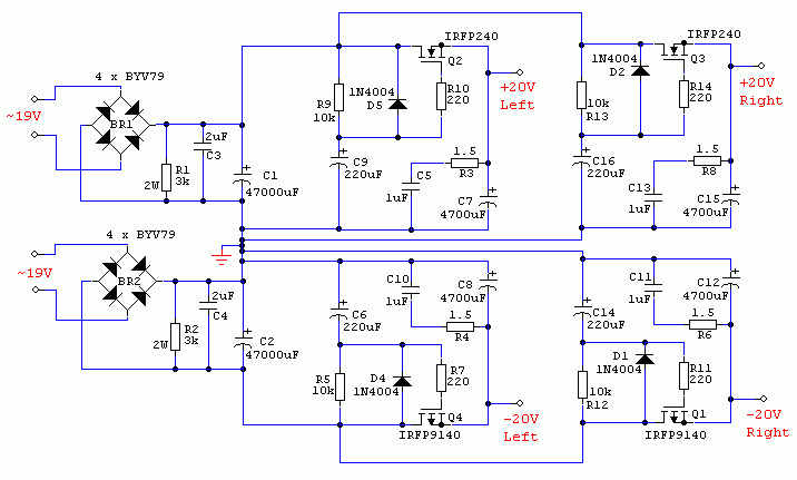
Where is R15? There is a 1.5R resistor that appears to be a snubber with 1uF. I don't see any 1.5k resistor ?
Hi xrk971,
1 - Are all resistors 1/4w - 1/2w except the ones specified?
2 - What's the maximum input and output voltage of this circuit (aside using the proper capacitor voltage).
3 - What is the maximum current that we can draw from this circuit?
Thinking of maybe using it for some Class A amplifiers
Thanks
Do
It's not my circuit so Juma would be the one to ask. But, given that it uses a beefy IRFP MOSFET it would seem that it can handle up to max rating of IRFP240/9240. That would be 200V and continuous current of 12 amps. It's ability to smooth ripples though would need tone modified with different parts of you plan on running it higher currents. Juma designednit for the F5 which is circa 1.5amps. I used 0.5w on 220R and the 1.5R and made by paralleling qnty. 0.25w 6 x 10R's (1.5w). Although I think 0.5w is probably fine. I definitely used it for a class a amp at 1.5 amps and it worked fine. I made 10k from two 4.7k in series so all my resistors were at least 0.5w.
Last edited:
Hi
I just wanted to say thanks to the people who took the time to have a look and reply to my first attempt at a layout.I`ve got a couple of things that transpired over the preceding weekend that brought about a change of direction.I also went over the layout and found a couple of errors,much to my own embarassment.Oh,the shame of it.
Trying to post via my cellphone seems to be nightmare(less than 5% success rate-normal quick replies seems to be ok) especially when you want to add attachments.I have been trying to post since Tuesday.I am posting from a desktop pc at the moment.
I had a look at all the available layouts,of which the last one(dacz) had all the changes mentioned in the thread.Also took a look at other layouts for guidance.This is tough layout,very "tight",especially if you are starting out.I went through a couple of revisions after my "blunder" which brought me to the current one.Thanks guys for being "diplomatic" regarding my misguided intentions.
I have a couple of people to respond to,who replied with ecouragement,advice and such.
1.gannaji:I am glad you liked the layout but unfortunately,as mentioned above,it is riddled with errors and inconsistencies.I have not abandoned the 100x50mm layout(you wil see something very soon).Have a look at the one i am posting now to have an idea.
2.xrk971: mentioned "something different".i`ve taken a lot of design cues and tried to incorporate it into my layout.I think it came out ok,plus it was good mental exercise as well.Regarding trying a proven layout,i concur,is usually best.But in the spiriy of diy i thought it would be ok to try my hand at a layout and post in this thread.I am learning still,but have a look and give your opinion.Any advice or opinion is a learning tool,whether good or bad.
3.evanc:i have taken your advice and made some changes,especially lead spacing of the resistors.It seemed to have helped with the layout as well.
If there is some other questions regarding the new layout,i will explain in detail if there is interest in it.I have included a zip with layout options.
Please guys,a second set of eyes does help a lot,and no beginner can compete with an experienced mind and eye.
Righto...here we go again.
Attachments
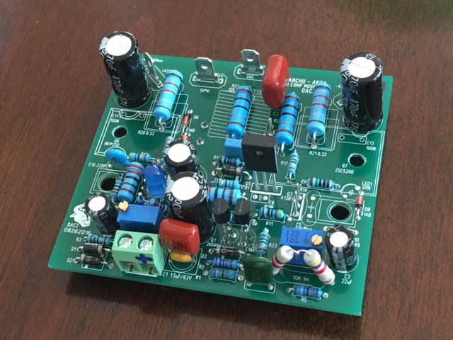
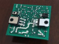
Almost done with new Dacz board. I made a few minor substitutions like 0.22R source/collector resistors and used SMT 100nF bypass caps on underside. Also 22pF NP0 SMT instead of 30pF mica. Using NJW output rather than 2SC5200. Still needs the output inductor to be rolled. It's a nice board and easily soldered with enough clearance in most places. Am I going to run into any issues with a 500R trimpot for setting offset vs spec'd 200R?
Attachments

Last edited:
Looks good.
500r for the offset trim pot is what I used. It is set close to center. I used a 5K pot for the bias trim. It is what I had. Works OK but the adjustment happens all in a few turns...a bit touchy.
500r for the offset trim pot is what I used. It is set close to center. I used a 5K pot for the bias trim. It is what I had. Works OK but the adjustment happens all in a few turns...a bit touchy.
I just fired it up and the bias pot and DC offset pot all work well. Able to get steady 100mA bias and 2 or 3mV offset. I must have a resistor off somewhere because sound is not loud. The gain is way low. On base of BJT output calls for 2R2 which I don't have so I put a 10R there. Wonder if that could be throwing it off? No magic smoke or anything at least and it trims nicely though.
I think I found the problem: R10 should be 68k but I have 680R. It's amazing how often this happens to me on almost every build. 😛
Congratulations, Z!
Do you think it sounds better than your proto?
BTW, raise one end of R10, then have a listen. Then reconnect and listen again. Please let us what you notice!
Hugh
Do you think it sounds better than your proto?
BTW, raise one end of R10, then have a listen. Then reconnect and listen again. Please let us what you notice!
Hugh
Last edited:
That pesky 68k R10 was the problem. Unit #1 is singing nicely. 🙂 Sounds great.
Te be honest, I can't tell any difference with one speaker playing and only 5 songs so far. What is true is that the circuit layout works perfectly with the specified values. The bias trim is infinitely adjustable and very stable. It seems that the BD139 tempco mounted on the heatsink nearby is doing a fine job. The zero DC offset trim works perfectly too - a lot of range and hits zero easily. Stable within +/- 15mV once warmed up. I think I am seeing power supply ripple. If I used my Juma Easy Peasy cap multiplier, I bet that DC offset ripple would zero.
Do you think it sounds better than your proto?
Te be honest, I can't tell any difference with one speaker playing and only 5 songs so far. What is true is that the circuit layout works perfectly with the specified values. The bias trim is infinitely adjustable and very stable. It seems that the BD139 tempco mounted on the heatsink nearby is doing a fine job. The zero DC offset trim works perfectly too - a lot of range and hits zero easily. Stable within +/- 15mV once warmed up. I think I am seeing power supply ripple. If I used my Juma Easy Peasy cap multiplier, I bet that DC offset ripple would zero.
Both Channels Working Now
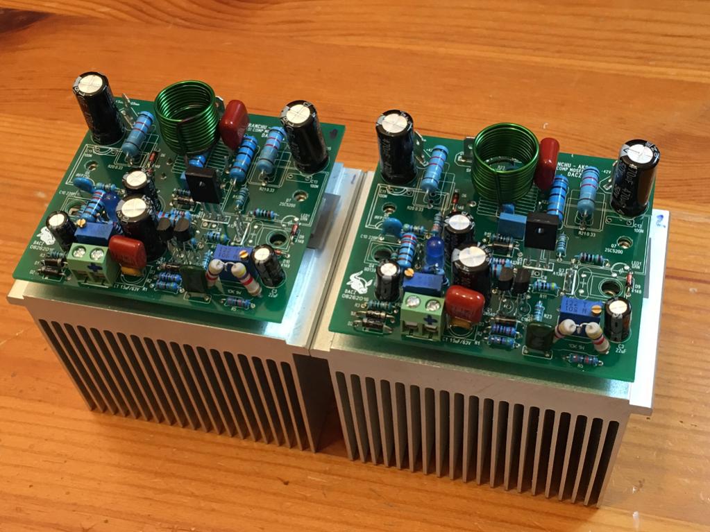
The Dacz boards are both completed and tested. Setup was smooth and easy on both. An excellent board that is easy to build. At 100mA bias (35v rails), I do not need a fan for the little Pentium heatsink that I am using. Very compact hifi setup. Sounds fantastic - long term listening and some speaker measurements next and I will report back with overall impressions. I am using higher quality components so I expect the sound should be better - but you never know. These are also the Onsemi NJW0281G NPN outputs. Seems to be working very well though.
Absolutely a frustration free build and startup. The bugs on this can be definitively said to be "all worked out". Anyone should be able to take these Gerbers and BOM and have a good time now. 🙂
Hugh, what do you mean by raising one end of R10?
Attachments
Last edited:
Back side
In case anyone is wondering what the transistors look like on the backside etc - you can see where I mounted the tiny 100nF bypass SMT's. I think this should be standard on all layouts is to have some SMT pads across the through hole power caps for a small bypass. They are easy to do and save a lot of space on the top side (and they don't cost hardly anything).
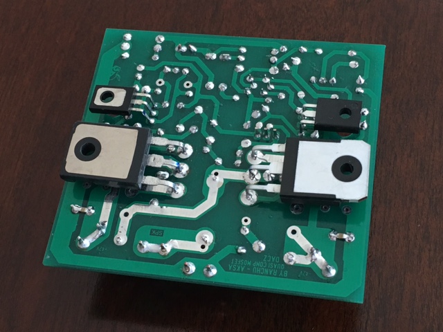
In case anyone is wondering what the transistors look like on the backside etc - you can see where I mounted the tiny 100nF bypass SMT's. I think this should be standard on all layouts is to have some SMT pads across the through hole power caps for a small bypass. They are easy to do and save a lot of space on the top side (and they don't cost hardly anything).
Attachments
- Home
- Amplifiers
- Solid State
- Very simple quasi complimentary MOSFET amplifier