Member
Joined 2009
Paid Member
Power Amplifier
So, following Christian's suggestion I swapped out R11 for a 1k resistor and then powered up with 20R in each power rail. This gave me the required bias adjustment range and I set the outputs so that I measured 52mV from emitter (NPN) to emitter (PNP). It drifted up to 56mV over a minute or so and then stabilized there as the heatsink heated up over 10 to 15 minutes.
I'd prefer if it had drifted down. It suggests that with 1k we're on the edge where the temp. co. of the Vbe multiplier is matching that of the output devices. Should give best accuracy and if Christian says he didn't blow up any amps with these values then I'm good with that.
Some observations: this amp runs warm, with around 100V rail-to-rail there's a lot of dissipation going on.
The VAS and two driver transistors get noticeably warm to the touch. I measured 7.8mA through the drivers (from voltage drop across R15, their shared resistor). I measured 9.1mA through the VAS (from voltage drop across R6, the 'constant current' bootstrapped resistor).
The dc-protection circuit is drawing 15mA through the LED as measured from the voltage drop across R32 which is 50% higher than I want. I found R32 was bordering on hot.
The dc-offset was 68mV out of the gate, with the adjust pot in mid-range. I ran out of range on this, with minimum resistance getting it to 37mV. I didn't check LTP balance yet but some further resistor changes will be needed.
I've not had this many mismatched-to-simulated behaviour before, but simple enough to fix on the bench.
p.s. turns out my solder sucker is gold coloured 😀
Last edited:
I've never blown anything up because of that 🙂
I should have mentioned that it is my usual practice to mount the thermal sensor directly on top of one of the output transistors, where it will track closely and react quickly to temp changes. I think what you have observed is normal and I usually make final adjustment once the temp has stabilised after about 15 mins.
If you want to return to the 1k5 then you require about 480R across the B-E junction; a 330R in series with that 200VR trimmer will do nicely.
change your VR to 500r or 1000rThanks for the formula...
So I have Rupper = 1,500R, Rlower = 220 to 420
Max output = 1500/220 +1 = 7.8 Vbe
Min output = 1500/420 +1 = 4.5 Vbe
hmmmm, the minimum output seems borderline for double EF, would be better if it were closer to 3.5 Vbe. I'll probably try changing the ratio when I get back tonight.
and maybe change the 220r (fixed) to 270, or 300, or 330, or 360 depending on the maximum output voltage you want across the drivers.
A triple EF should never need more than about 7*Vbe, depending on the Tj of the various devices. A double EF should be limited to <~5Vbe, again depending on device temperatures.
An external sensor will never track Tj accurately and never track deltaTj quickly.............................
I should have mentioned that it is my usual practice to mount the thermal sensor directly on top of one of the output transistors, where it will track closely and react quickly to temp changes. ..............
You are kidding yourself to think so.
The best you can do with an external sensor is to track slow changes that are a proportion of the delta Tj. That proportion may be only 50% to 70% of the actual device temperature change.
You compensate for that by applying a multiplying factor greater than 1. But it will still remain a slow correction.
D.Self talks about it and R.Cordell goes into a bit more detail. They both agree that external sensing is slow and under compensates requiring that multiplication. Both make suggestions to try to reduce the slowness of the monitoring.
The multiplication comes form the sensor monitoring the output devices (2 Vbe in series) and the unmonitored Drivers (another 2 in series) that hardly change temperature when a substantial heatsink is used.
Apply a 4Vbe muliplier to the combined drivers plus outputs. Change the output temperature and hold the drivers at a constant temperature and the arrangement effectively applies a multiplication factor of 2times to the delta Tj of the outputs. If the sensor moves 50% of the delta Tj, then the compensation is just about correct.
Can you point me to the schmeatic you are using, so I can see what the arrngement is.
Last edited:
Andrew, what I meant to say and probably should have said is that by placing the thermal sensor atop an output transistor, it will *more* closely track and *more* quickly react to temperature changes when compared with the more common scheme, which is to fix the sensor to the heatsink an appreciable distance from the output transistors.
Can we agree on this point and move on? It is tiresome in the extreme to have to guard and qualify every statement on a forum for light-hearted chit-chat between hobbyists, not "serious" discussions between engineers and academics.
The schematic I'm referring to is the one posted by Bigun, based on AKSA 55.
I'm familiar with some of the more elaborate schemes with two semiconductors, which allow the designer to obtain different ratios of compensated and uncompensated spread. I've never found this necessary in most cases, but have applied the technique in couple of vertical mosfet projects where I used two inexpensive bipolars in the bias generator to obtain a "good enough" ratio of compensated bias.
I think Bigun has made it pretty clear that this thread is for discussion about his adaption of the Hugh Dean design and not to enter into debate about possibly "improvements" to the circuit. I think the basic spreader has been proven in the AKSA circuit and the myriad of other bipolar EF2 designs.
Agreed that "closer" is an appropriate description.
A change of resistor value to give a range of adjustment is hardly an "improvement" when all it should do is allow the correct adjustment to be obtained.
If the original choice of values does not allow the correct adjustment to be obtained, then the amplifier is effectively "broken" and requires repair to bring it up to specification.
Agreed, but in #144 you appeared to be steering the discussion towards some of the more elaborate compensation schemes that Cordell discusses in his book and elsewhere; my apologies if that was not your intention.
But it was really your comment "you are kidding yourself" that got my back up 😀
What you posted was completely wrong. Beginners reading your post would be misled.
That's why I felt the need to correct your erroneous statement.
As for the following explanation of tempco compensation, that was provided because Bigun seemed not to understand why he was not able to adjust his amplifier.
I am not trying to modify the amplifier. Just to provide sufficient information so that he is able to make the correct adjustment.
He has since made a change
and follows withSo, following Christian's suggestion I swapped out R11 for a 1k resistor and then powered up with 20R in each power rail.
implying that he misunderstood the mechanism at play.I'd prefer if it had drifted down. It suggests that with 1k we're on the edge where the temp. co.
Last edited:
Member
Joined 2009
Paid Member
A change of resistor value ....... all it should do is allow the correct adjustment to be obtained.
My way of thinking may be wrong but I've always thought that the choice of resistor values does two things - the total resistance of the bias string establishes the sensitivity of the Vbe to temperature changes. The ratio of upper and lower resistor values in the bias string establishes the adjustment range but not the sensitivity to temperature.
My reasoning for why the bias string total resistance affects the temp co is because the current flow through the Vbe multiplier is constant (bootstrapped 'current source) but split down two parallel paths, one through the BJT and the other down the resistor bias string. The more current that flows down the bias string (which is not a temperature sensing element) the less current flows through the BJT (the temperature sensing element) so overall the bias generator is less sensitive (lower multiplier in your language).
So if I were to increase the upper resistor back to 1k5 and increase one of the lower resistors to maintain the required adjustment range I would reduce the total current though the bias string and increase it through the Vbe multiplier - this would increase the multiplication factor and the Vbe multiplier would slightly over-compensate but therefore be safer.
In practice, the bias did stabilize after a couple of minutes and remained solid for at least quarter of an hour (albeit with no input signal and no load). What made me nervous was the fact it drifted up 4mV before it stabilized so I may make further changes.
The Vbe multiplier BJT is mounted directly on top of, and in good thermal contact with, one of the output devices. I too prefer this approach for all the reasons mentioned above.
Last edited:
that is not the way the Vbe multiplier works.
As I said it is a shunt regulator.
The output voltage is a factor times the transistor's Vbe.
If that transistor is thermally connected to a sense point, then the Vbe will change with changes in the sensor Tj.
The proportion of current through the resistor string has almost no effect on the output voltage.
Where the current through the resistor string does matter is in what part of that is drawn to the base of the transistor. That current draw creates an error.
Take a resistor string that pulls 1mA and the remaining 5mA of a 6mA VAS+CCS will pass through the multiplier and the drivers of the next stage.
If hFE is 100 and the transistor Ic=4.5mA, then the base current will be 45uA
That base current is pulled out of the resistor string, making the upper resistor current slightlly more than the lower resistor current. 1mA in the upper resistor and 0.955mA in the lower resistor. There's the voltage ratio error of the resistor ladder.
That does not affect the tempco.
The voltage ratio+1 times the Vbe stays the same whether 45uA passes as base current, or 10uA, or 100uA. The voltage ratio changes very slightly but the Vbe is still the temperature related tempco.
one bit of guidance for the multiplier. Don't let the base current into the transistor become more than 10% of the string current. The voltage ratio error starts to become bigger as you approach 10%. The ratio error is much lower if base current is only 1% of the string current. A bc550C with an hFE of 450 drawing 5mA will have a base current of 11.1uA
A dual EF multiplier set to 4Vbe having 2mA passing down the string will give <0.6% drawn from the string. That 2mA will be due to the lower resistor set to ~300r and the upper resistor fixed at 1k
Changing that to 2k & 600r reduces the string current to ~1mA and the base current is still ~1.1% of the string current. The ratio error using a C grade bc550 (or sot23 bc850c) is ignorable.
And don't ignore the current draw of the drivers. It affects the multiplier current. Worse for a dual EF driving 4ohms, almost imperceptible for a triple EF driving 8ohms.
Last edited:
Member
Joined 2009
Paid Member
As I said, my thinking may be wrong ! - I had in mind the extreme case where if the resistor string was very low impedance it will begin to 'shunt' the BJT device and dominate the behaviour. Perhaps that's too much an extreme and doesn't figure into the considerations here.
Gee... I was really enjoying this thread up until the last couple of pages. I don't know about the rest of you, but I could do with more photos and interesting updates from Bigun and less arrogant lecturing from a certain other participant. This forum has an ignore feature, perhaps it's time to put it to good use.
Member
Joined 2009
Paid Member
I'll get some more photos 🙂 progress isn't so easy for me these days as I have significant family obligations - looking after a pair of teenagers with school pressures the poor things !
But I really don't mind some debate, I do like to learn what others have to say - I'm very tolerant to the style of different posters if we are focused on the technology. I particularly value very much your contributions Christian.
But I really don't mind some debate, I do like to learn what others have to say - I'm very tolerant to the style of different posters if we are focused on the technology. I particularly value very much your contributions Christian.
Member
Joined 2009
Paid Member
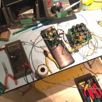
I was able to make a bit more progress tonight. I swapped out R4, the LTP load resistor for a 1k ohm value which sorted the dc-offset (to around zero mV). My Spice simulations were off thanks to a poor model for BD139, not sure how much more 'damage' this has caused or how I ended up with a different model than I've used for past projects.
I measured the LTP current balance, getting 551uA through R4 and 585uA through the other leg. The difference is 34uA which is of course, the base current for the VAS. Given that the VAS is running at round 8mA the beta of the VAS must be around 235 which seems quite reasonable.
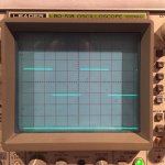
I hooked up the scope. Using the scope-probe test signal (1kHz 500mV p-p) I was able to observe a clean square wave at the output with & without an 8R resistive load. The gain appeared to be around x24 or 27.6dB - have to check as this seems a bit higher than expected.
After removing the power rail safety resistors I played some music through a B&W floor standing speaker using an iphone 6 as the source. It was not a great quality source (itunes, probably mp3) hence although the sound was there it was not hi-fi by any means - wiring was not optimal and iphone was not ideal but I wanted to hear music! I shall have to explore further to ensure the sound is good before I do more as my ears are the only distortion meter I have in my laboratory and I didn't like what I heard nearly enough to be happy.
The main heatsink was warm after all that work, the bias had drifted up slightly to around 60mV but was stable at this elevated temperature. The VAS and drivers were all quite hot. As I could hold a finger on them still my guess is that the temperature was around 50degC which is OK.
The resistor feeding the output opto-isolator LED was also hot to the touch, I'd estimate around 60degC. It's dissipating 90% of it's nominal rating (1/4 W) and I'm not happy with this - I raised the resistor clear of the pcb surface so that it had more air around it - I don't have any higher wattage 1k resistors to put in there at present but ideally a 1/2 W rated resistor should be installed.
I measured the LTP current balance, getting 551uA through R4 and 585uA through the other leg. The difference is 34uA which is of course, the base current for the VAS. Given that the VAS is running at round 8mA the beta of the VAS must be around 235 which seems quite reasonable.
I hooked up the scope. Using the scope-probe test signal (1kHz 500mV p-p) I was able to observe a clean square wave at the output with & without an 8R resistive load. The gain appeared to be around x24 or 27.6dB - have to check as this seems a bit higher than expected.
After removing the power rail safety resistors I played some music through a B&W floor standing speaker using an iphone 6 as the source. It was not a great quality source (itunes, probably mp3) hence although the sound was there it was not hi-fi by any means - wiring was not optimal and iphone was not ideal but I wanted to hear music! I shall have to explore further to ensure the sound is good before I do more as my ears are the only distortion meter I have in my laboratory and I didn't like what I heard nearly enough to be happy.
The main heatsink was warm after all that work, the bias had drifted up slightly to around 60mV but was stable at this elevated temperature. The VAS and drivers were all quite hot. As I could hold a finger on them still my guess is that the temperature was around 50degC which is OK.
The resistor feeding the output opto-isolator LED was also hot to the touch, I'd estimate around 60degC. It's dissipating 90% of it's nominal rating (1/4 W) and I'm not happy with this - I raised the resistor clear of the pcb surface so that it had more air around it - I don't have any higher wattage 1k resistors to put in there at present but ideally a 1/2 W rated resistor should be installed.
Attachments
Last edited:
Member
Joined 2009
Paid Member

Gareth, my 2 cents, based on my hybrid experience - best noise / hum performance has been shown, when both 6.3V AC wires were shunted to ground with 0.1uF capacitors (close to the PSU).
Cheers,
Valery
Cheers,
Valery
Member
Joined 2009
Paid Member
I like that idea Valery - darn, I would have been able to add that to the pcb but too late for this version - nevertheless I'm sure I can tack on a couple of capacitors without harm.
Gee... I was really enjoying this thread up until the last couple of pages. I don't know about the rest of you, but I could do with more photos and interesting updates from Bigun and less arrogant lecturing from a certain other participant. This forum has an ignore feature, perhaps it's time to put it to good use.
You said it! My ignore is selected. 😡
Gareth, I have quietly followed your design from your first post - great stuff guy.
Hi Nico,
Perhaps we are seeing Dunning-Kruger?
He means well......
Gareth, congratulations on your latest!
Hugh
Perhaps we are seeing Dunning-Kruger?
He means well......
Gareth, congratulations on your latest!
Hugh
- Status
- Not open for further replies.
- Home
- Amplifiers
- Solid State
- TGM 1i - an integrated hybrid amp inspired by Hugh Dean