
Hello Ranchu32
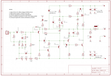
greetings how important is C5 33pf silver mica in this amp hard to find
33pf silver mica in my place
warm regards
Andrew
greetings how important is C5 33pf silver mica in this amp hard to find
33pf silver mica in my place
warm regards
Andrew
Hi Ranchu and AKSA ,
It would be a bad idea to put PSU CAP PCB amp ?
Any idea ?
Best Regards
Its a good idea to put the bulk decouplers on the PCB. 10,000uF caps are excessive. You would be more economical and improve performance if you used 4,700uF caps and insert some small R's (about 100mohm to 220mohm) to create a CRC supply
This layout you've done looks beautiful, but I worry about noise and hum with the bulk caps on both sides of the board. As you know, with a Class B amplifier, the output stage pulls heavy currents from each rail on alternating half-waves. This will result in heavy current through the ground trace, which runs across the board and very near the input stage, which is particularly sensitive to these disturbances. The ground lift will help to some extent but improved ground routing would be better.
Hello Ranchu32
greetings how important is C5 33pf silver mica in this amp hard to find
33pf silver mica in my place
warm regards
Andrew
A quality NP0/C0G multilayer ceramic can be used instead. Please Avoid single layer or X5R/X7R dialectics as these will kill the sound.
Hi Guys
Mosfets tend to be more nonlinear at low idle currents, plus the circuit is highly asymmetric requiring higher idle to achieve reasonable performance.
I would suggest that the CRC supply idea be abandoned. It is good to have large local filters, and the use of multiple filters rather than single large filters is favourable. Keeping the supply impedance low over the audio band is preferred, even though there are examples from pass, Cherry, and others using CRC and CLC supplies. Those tend to be for class-A amps, or in Cherry's case, to enhance stability of a layout that might have marginal stability.
Have fun
Hi Terry
Current schematic including set up notes. It may be necessary to experiment with R5 if it is found that there is insufficient range of adjustment on VR1 to trim the offset.
Regards
Christian
Can someone point to the PCB that goes with this schematic?
Post #333 or use post #380 by diacomogi.Can someone point to the PCB that goes with this schematic?
Last edited:
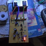
i have been thinking if using a N Fet to replace the NPN power transistor and driver, retaining the PNP output and low side driver.
the bias needs to go to about 4.5v to start conduction.
Does anyone know what the distortion is?
the bias needs to go to about 4.5v to start conduction.
Does anyone know what the distortion is?
Any answer?D8,C9,R19 back in position.
Now the Vbe multiplier is in normal conditions.
Trying to figure the distortion graph i see that one channel have a lower distortion than other. Same idle current,same offset,same levels,same power supply.
Duple checked.
Is this as a matter of transistors hfe ?
Yes, but it could easily be a minor issue with ground impedance too. Very critical to THD, but, and note this, YOUR EAR WON'T NOTICE!!
Cheers,
Hugh
Cheers,
Hugh
Thiagomogi,
Please don't be upset because the other guys are fascinated by the technical aspects!
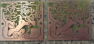
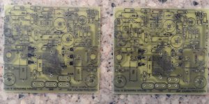
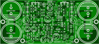
Personally, I think you have done a beautiful pcb, along with Prasi, yours is perhaps the best I've seen and arguably better than I did on the FetZilla, so take a bow, and thank you for your expert efforts! Here attached is your layout to refresh our memory.
The technical issues are very interesting and bring up philosophy, engineering, experience, and BOM costs. But the layout takes the most time, in my experience, I usually spend about 50 hours on mine. Design is done in inspirational moments, slowly from a well known base. After you'd done your 10,000 hours in this game, designing a new amp focusses on two or three small details and concepts and the other issues are sketched in very quickly from experience. My NAKSA 70 took about three weeks, the 80 came after a few days, on table napkins in coffee shops, and just recently, the SAKSA 80 drawn on inspiration with speed from the NAKSA, the Maya, and the original AKSA from 2000. The design took a few days, but the layout took about two months. So, in terms of the efforts, the design is inspirational, enjoyable and quick; but the layout is hard, difficult work, particularly if you need to use brand new components you have never used before.
So, guys, let's thanks Thiagomogi for his brilliant pcb design!
Cheers,
Hugh
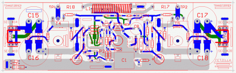
BTW, Christian, I agree, the FetZilla design would work extremely well and is fairly compact. Here is the pcb.
HD
Please don't be upset because the other guys are fascinated by the technical aspects!
Personally, I think you have done a beautiful pcb, along with Prasi, yours is perhaps the best I've seen and arguably better than I did on the FetZilla, so take a bow, and thank you for your expert efforts! Here attached is your layout to refresh our memory.
The technical issues are very interesting and bring up philosophy, engineering, experience, and BOM costs. But the layout takes the most time, in my experience, I usually spend about 50 hours on mine. Design is done in inspirational moments, slowly from a well known base. After you'd done your 10,000 hours in this game, designing a new amp focusses on two or three small details and concepts and the other issues are sketched in very quickly from experience. My NAKSA 70 took about three weeks, the 80 came after a few days, on table napkins in coffee shops, and just recently, the SAKSA 80 drawn on inspiration with speed from the NAKSA, the Maya, and the original AKSA from 2000. The design took a few days, but the layout took about two months. So, in terms of the efforts, the design is inspirational, enjoyable and quick; but the layout is hard, difficult work, particularly if you need to use brand new components you have never used before.
So, guys, let's thanks Thiagomogi for his brilliant pcb design!
Cheers,
Hugh
BTW, Christian, I agree, the FetZilla design would work extremely well and is fairly compact. Here is the pcb.
HD
Attachments
Last edited:
WOWWW this is a great encouragement to me Hugh . thanks for nice words . I will strive more and more to improve .
Best Regards
Best Regards
WOWWW this is a great encouragement to me Hugh . thanks for nice words . I will strive more and more to improve .
Best Regards
Yes, the curvy design of tracks and layout is too good. Also your AX-11 design all with unique straight tracks is beautiful. I hope I am able to do as good as you.
reg
Prasi
Thiago,
I take my hat off to you, Prasi, and Alex MM. You three bring good ideas on this forum into layout reality; we need to foster this, along with incredible work from Terry, Thimios, Christian, Kevin, XRK and many others who build and listen........
We are very lucky to have you and others.
Hugh
I take my hat off to you, Prasi, and Alex MM. You three bring good ideas on this forum into layout reality; we need to foster this, along with incredible work from Terry, Thimios, Christian, Kevin, XRK and many others who build and listen........
We are very lucky to have you and others.
Hugh
- Home
- Amplifiers
- Solid State
- Very simple quasi complimentary MOSFET amplifier