I don't keep a register/index of designs.
Why? The life is short!
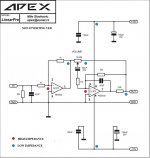
This amp need preamp or buffer on input, it can not work only with pot, use this preamp for A2 or any other amp.
Preamp use standard psu +/-15V ref to gnd not to amp out.
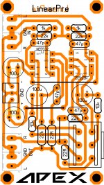
I tried to draw a layout. Can someone check it? A couple of things to note. I swapped the 10k/100u to make the layout easier. They are in series so hopefully that won't matter. Also, the 100n will be SMD on the bottom of the board.
Thanks, Terry
Attachments

Last edited:
I swapped the 10k/100u to make the layout easier. They are in series so hopefully that won't matter.
The first thing I would do when creating layout for circuit like this, is to put the two feedback resistors very close to the input pins (the 47p or lower underneath). The 22k is for sure has to be placed close to the input. The 10k as well (it is somehow connected to the output).
I tried to draw a layout. Can someone check it? A couple of things to note. I swapped the 10k/100u to make the layout easier. They are in series so hopefully that won't matter. Also, the 100n will be SMD on the bottom of the board.
Thanks, Terry
Nice work,
Regards
Attachments
The first thing I would do when creating layout for circuit like this, is to put the two feedback resistors very close to the input pins (the 47p or lower underneath). The 22k is for sure has to be placed close to the input. The 10k as well (it is somehow connected to the output).
I agree. And I will put 100nF decoupling, very close to power pins of the IC.
I tried to draw a layout. Can someone check it? A couple of things to note. I swapped the 10k/100u to make the layout easier. They are in series so hopefully that won't matter. Also, the 100n will be SMD on the bottom of the board.
Thanks, Terry
If you rotate the two 100uF rail caps 180 degrees, you can eliminate the the ground trace lengths.
The first thing I would do when creating layout for circuit like this, is to put the two feedback resistors very close to the input pins (the 47p or lower underneath). The 22k is for sure has to be placed close to the input. The 10k as well (it is somehow connected to the output).
Still4,
Take into account good Jay, Bimo, Jwilelm`s suggestions, also look at non-inverting version of this nice LinearPre. There are marked low/high impedance points.
Make shorter as possible the connections to the high imp. pins (IC inputs),
the low impedance pins (IC outputs) can be longer as the outputs tends to achieve virtual GND with very low impedance values.
Cross signal and power lines perpendicularly to each other, to avoid inducted/transform. undesirable effects.
Avoid PCB GND loops
PS to ICs: Decoupling, Decoupling, Decoupling 🙂
Attachments
Last edited:
I suppose I should wait until one of you has time to do a layout. That took hours and obviously has several flaws. I'm not experienced enough to understand your suggestions.
Thanks, Terry
Thanks, Terry
I suppose I should wait until one of you has time to do a layout. That took hours and obviously has several flaws. I'm not experienced enough to understand your suggestions.
Thanks, Terry
The layout isn't terrible. You are getting much better at it. No matter how much time you spend on it, there's always room for improvement.
When dealing with op amps, or any other IC for that matter, you always place small(.1uF) decoupling caps right beside the feed pins to reject any noise from the power supply rails. Feedback components should to be as close to the input as possible too, because of capacitance and resistance in the pc board traces.
Last edited:
The layout isn't terrible. You are getting much better at it. No matter how much time you spend on it, there's always room for improvement.
When dealing with op amps, or any other IC for that matter, you always place small(.1uF) decoupling caps right beside the feed pins to reject any noise from the power supply rails. Feedback components should to be as close as possible too, because of capacitance and resistance in the pc board traces.
Hi Jeff,
I don't see those decoupling caps on the schematic so I don't have a clue what you mean. I knew I was taking a big risk trying to do this layout but I wanted to build it. Maybe someone who knows how will take an interest and make one. It was good practice if nothing else.
Blessings, Terry
Decoupling caps aren't always on the schematic, but they should be. If you look at any of the Slewmaster layouts with op amps for example, you will see .1uF caps on the op amp + feed and - feed.
These caps are low pass filters' just like the 150pF cap on an amplifier input. They filter out any high frequency garbage from the power supply rails.
These caps are low pass filters' just like the 150pF cap on an amplifier input. They filter out any high frequency garbage from the power supply rails.
Decoupling caps aren't always on the schematic, but they should be. If you look at any of the Slewmaster layouts with op amps for example, you will see .1uF caps on the op amp + feed and - feed.
These caps are low pass filters' just like the 150pF cap on an amplifier input. They filter out any high frequency garbage from the power supply rails.
So do they go between pin 4 and pin 8?
Yes. There's still a lot of disagreement on the proper way to do it, but when there are separate positive and negative rails, I normally would put one from pin 4 to ground, and another from pin 8 to ground. Some argue that it should be a single cap between pin 4 and pin 8. You could do this with the layout you have, by tacking one on under the board right on the pins.
Last edited:
Ok, I guess those are on the schematic. I assumed they were there to decouple the electrolytics so I placed them under the board right on their pins. Guess I need to start over.
It doesn't hurt to put them all over the place. I like to put them on every IC and right at the supply connector to the board.
It doesn't hurt to put them all over the place. I like to put them on every IC and right at the supply connector to the board.
Ok, I will check out your Slewmaster layouts for examples. TI recommends ceramic so I may try locating smd on the underside.
I suppose I should wait until one of you has time to do a layout. That took hours and obviously has several flaws. I'm not experienced enough to understand your suggestions.
Thanks, Terry
Do not give up. It take 2 years for me as young engineer to make good PCB layout at my first professional carrier. Even, it take longer to understand how to design a good audio circuit.
I suppose I should wait until one of you has time to do a layout. That took hours and obviously has several flaws. I'm not experienced enough to understand your suggestions.
Thanks, Terry
Terry your pcb is not perfect but preamp will work fine with this layout.
Regards
- Home
- Amplifiers
- Solid State
- 100W Ultimate Fidelity Amplifier