central point for gnd is 3116, gnd for smd's have toptraces going back to 3116 where they go to gnd bottomlayer pcb, electrolytics are directly soldered to bottomlayer
bypassing versus decoupling
bypassing versus decoupling
I mentioned creek and the article to note the source of why I looked at this. I am not suggesting to copy their designs, but it did make sense looking at my board, and the 3116 schematic.
I think mine must have the star ground as no traces go from any IC gnd's, but as that isnt on data sheet schematics I don't really know much about that part of circuit, and definately not going to lift IC. But there is a trace coming out from under IC to the "bypass caps" positive trace, and returns to electrolytic negative on the 1nf/100nf side of board.
The drawings I posted are based on my board circuit and the 3116 schematic, the creek article had no drawings. The fact that the 1nf positive side is nearer to pvcc input than 100nf yet the opposite on return to electrolytic negative trace on board forms a "loop" in the circuit, and means both the 1nf and100nf does and doesn't bypass the electrolytic < that's difficult to explain, apart from the trace going from under IC to electrolytic. I also don't see any traces from the 100nf to under the IC.
I am more confused now!!!!! lol.
No mention of YuanJing in there. yuan jing audio website does not show this board, looks like YJ copies whatever they like and now some others started copying YJ LOL
seller i got from listed as "official" as well. the yj site had them reduced as well, might have well as spent the extra few dollars to order from official site instead.
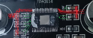
anyhow, another one of my "dodgey" drawings. this is, as far as I can tell the smd "bypass caps" circuit I can see on both these boards.

you can see what I mean with the nearest bypass cap to pvcc being furthest from return to electrolytic, but the nearest returning neg to the electrolytic is not the nearest to it on positive trace. Thus forming the "crossed" caps in the electrolytic bypass.
central point for gnd is 3116, gnd for smd's have toptraces going back to 3116 where they go to gnd bottomlayer pcb, electrolytics are directly soldered to bottomlayer
bypassing versus decoupling
but mine do have traces going from electrolytics through bottom smd to 3116 star ground as well!
regardless of whether the ground returns to electrolytic or 3116 starground, the smd's still from a "cross in the circuit dont they?
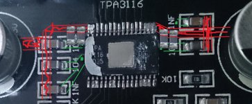
anyhow, another one of my "dodgey" drawings. this is, as far as I can tell the smd "bypass caps" circuit I can see on both these boards.
View attachment 489326
you can see what I mean with the nearest bypass cap to pvcc being furthest from return to electrolytic, but the nearest returning neg to the electrolytic is not the nearest to it on positive trace. Thus forming the "crossed" caps in the electrolytic bypass.
Sorry but i dont get it. 😀 The 1nF's return-GND is the IC-Gnd. Positive and negative "leads" from this cap should be equal in length. If not possible, positive should point to the IC. Loop areas should be minimized. This is just a high-frequency bypass.
Suppose its whether you want them operating in parallel to both dc power cap and eaxh other OR just in parallel to each other.
central point for gnd is 3116, gnd for smd's have toptraces going back to 3116 where they go to gnd bottomlayer pcb, electrolytics are directly soldered to bottomlayer
bypassing versus decoupling
OK. Gonna leave this one. But looking at it has caused a little confusion to me regarding the side with the 10nf cap and traces to under the 3116.
Where the 10nf is nearest pvcc pins, there looks to be 2 very close together, very narrow traces from the 3116 side of the 10nf to under the 3116.
Are these going to star ground? I can't in my head see how they are as they are on same side of the smd cap as the pvcc pins. Wouldn't that just pass pvcc straight to ground, instead of through the high freq bypass caps?
There is also a trace on other side which goes from under 3116, between the middle 100nf cap and the 10k resistor, to the electrolytic neg.
Starting to think I need to find another $35 and buy replacement board from YJ website.
silly green dots are vias, electrolytic positives have a pcbtrace bottomside connecting them, which is located under tpa3116 silkscreen text topside
Attachments
Last edited:
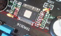
Yeah see. The red traces on your PIC are clearly visible as "raised" on my boards, but the one on right goes above the 1nf. Between the 104 & 10k, a trace runs from electrolytic to under 3116.
On the left of PIC, I can see a couple of tiny raised lines to the 10nf from under 3116. I don't see the 104, or 1nf having any raised traces going their.
As I said, my smd seem more "centered" to ends of 3116, and I think slightly closer. But from my "raised traces" which go from under 3116 to smd and from having 2 smd to electrolytics on both sides, I have a feeling the "star ground" on mine is also tied to electrolytic neg side by traces, at least on the right side of your PIC.
I'll get the multimeter out and check the trace flow again. Thanks for PIC of how YJ should be.
I recently bought what I thought was a YJ blue black from Amazon (listed as a HeroNeo) but it is different in that there is an LED and the bottom side has room for 3 SMT reverse polarity protection diodes, and the black paint on the bottom appears to have a cross-hatched silkscreen texture to it. The workmanship in general looks cleaner than my first YJ blue black. Is this the new version by YJ, or an improved knock-off of a knock-off of Danzz's board by yet another player? The parts are all blue (no white or yellow caps).
Amazon.com: HeroNeo® TPA3116D2 50Wx2 Official Version Finished Stereo Digital Power Amplifier Board: Electronics
I bought the same board from a different vendor. Before I bought it, I was suspecting it is not a YJ board since it has some different features. How do you like its sound? The reason I ask is because I was planning to mod this one but after a brief listen, I found the sound was very flat as compare to the SMKN board. I lost interest and it is still sitting on my work bench somewhere.
Just finished with multimeter. Pretty much as I drew before. I'll refer to your left PIC above.
On the right side with just 2caps, the + trace is above caps, it comes down into left side of top cap, then down to left side of bottom cap.
On the - side of top cap, the trace exits cap straight down to bottom cap - side, then down to a trace which extends all way from under 3116 to the - leg of electrolytic. It is this long trace which, along with the lack of vias you highlighted, that makes me think the 3116 star is returned to electrolytic - leg.
On the left side, the + trace to pvcc comes down to through the right side of all 3 caps in parallel. The - left side of these 3 caps all join and at the bottom cap the - returns to electrolytic - leg.
There are three slight differences compared to the right side. Obviously has 3 caps to include the 10nf as with yours.
2nd, the 100k resistor goes to the bottom cap on right + side
Third, there is a small trace, or two very tiny traces, going from top 10nf + to under 3116, but can't see a via. And this is the + side from the pvcc power line, so I can't see it going to GND anyway, as it would make the 3 caps null & void. Its where these two positive traces go which are now confusing me.
Last edited:
I bought the same board from a different vendor. Before I bought it, I was suspecting it is not a YJ board since it has some different features. How do you like its sound? The reason I ask is because I was planning to mod this one but after a brief listen, I found the sound was very flat as compare to the SMKN board. I lost interest and it is still sitting on my work bench somewhere.
I actually think it sounds OK. Pretty much same as the version I have been playing about with mods, when they were both stock. The only real difference in layout between my two is the under board diode xrk mentioned, and my other has connection for pentameter and rca plugs at input circuit.
I found the LED quite useful when using multimeter on traces to figure circuit layout, as it lights up when you bridge the + & - circuit.
That looks better than YJblue
That's it. Your a star.
Any idea why these two smaller traces would go under 3116 to back of pvcc as well as the pins on main trace? Is it to ensure the "flow" passes the 10nf instead of straight into pins!
I am presuming that ground going under 3116 from top electrolytic goes to star GND.
I suppose makers of these boards only put 10nf on that side because of the way the 3116 schematic shows it.
I'm going to strap a 10nf across the +/- on the underside to cover both channels.
Do you see what I mean now regarding the 1nf and 100nf crossing over each other in circuit order?
That looks better than YJblue
I ran across this info in another forum page the other day, which led me to examine this further. Can't remember where, or who it was by. But does seem to tie in with what my boards are doing:
"Good grounding is harder to explain than bypassing. It would take a whole book to really get into this issue, so I'm only going to mention pieces. The first job of grounding is to supply a universal voltage reference, which we usually consider 0V since everything else is considered relative to the ground net. However, think what happens as you run current thru the ground net. It's resistance isn't zero, so that causes a small voltage difference between different points of the ground. The DC resistance of a copper plane on a PCB is usually low enough so that this is not too much of a issue for most circuits. A purely digital circuit has 100s of mV noise margins at least, so a few 10s or 100s of uV ground offset isn't a big deal. In some analog circuits it is, but that's not the issue I'm trying to get at here.
Think what happens as the frequency of the current running across the ground plane gets higher and higher. At some point the whole ground plane is only 1/2 wavelength across. Now you don't have a ground plane anymore but a patch antenna. Now remember that a microcontroller is a broad band current source with high frequency components. If you run its immediate ground current across the ground plane for even a little bit, you have a center-fed patch antenna.
The solution I usually use, and for which I have quantitative proof it works well, is to keep the local high frequency currents off the ground plane. You want to make a local net of the microcontroller power and ground connections, bypass them locally, then have only one connection to each net to the main system power and ground nets. The high frequency currents generated by the microcontroller go out the power pins, thru the bypass caps, and back into the ground pins. There can be lots of nasty high frequency current running around that loop, but if that loop has only a single connection to the board power and ground nets, then those currents will largely stay off them.
So to bring this back to your layout, what I don't like is that each bypass cap seems to have a separate via to power and ground. If these are the main power and ground planes of the board, then that's bad. If you have enough layers and the vias are really going to local power and ground planes, then that's OK as long as those local planes are connected to the main planes at only one point.
It doesn't take local planes to do this. I routinely use the local power and ground nets technique even on 2 layer boards. I manually connect all the ground pins and all the power pins, then the bypass caps, then the crystal circuit before routing anything else. These local nets can be a star or whatever right under the microcontroller and still allow other signals to be routed around them as required. However, once again, these local nets must have exactly one connection to the main board power and ground nets. If you have a board level ground plane, then there will be one via some place to connect the local ground net to the ground plane.
I usually go a little further if I can. I put 100nF or 1uF ceramic bypass caps as close to the power and ground pins as possible, then route the two local nets (power and ground) to a feed point and put a larger (10uF usually) cap across them and make the single connections to the board ground and power nets right at the other side of the cap. This secondary cap provides another shunt to the high frequency currents that escaped being shunted by the individual bypass caps. From the point of view of the rest of the board, the power/ground feed to the microcontroller is nicely behaved without lots of nasty high frequencies"
I think I would drill some holes, vias to bottomgnd and cut gnd top traces to electrolytics, to think I improved the ampboard 🙂 I would also put 100nF in best position and add 10uF in second, and wouldn't care if there was a 1nF on one side still on pcb or not 🙂
Don't mind minor surgery, but that's beyond my comfort zone.
I was thinking of putting the left channel 1nf nearest pvcc, followed by 100nf, leaving off the 10nf by placing that across +/- underneath.
I was thinking of putting the left channel 1nf nearest pvcc, followed by 100nf, leaving off the 10nf by placing that across +/- underneath.
I bought the same board from a different vendor. Before I bought it, I was suspecting it is not a YJ board since it has some different features. How do you like its sound? The reason I ask is because I was planning to mod this one but after a brief listen, I found the sound was very flat as compare to the SMKN board. I lost interest and it is still sitting on my work bench somewhere.
I just got it a few days ago and have been rather busy getting my 200 watt $20 IRS2092 to work. Just got that finished last night with a proper Abltec 53v dual rail supply. Oh there is so much headroom with a big amp! It is very low distortion. Anyhow, back on topic. I have not had a chance to listen to it. It does look quite different visually and now StanleyB is pointing out all sorts of strange crossed vs star wiring on the bypass caps. I am actually not following this line at all? Aren't the traces from the two bypass caps to the Vcc pins so short, it doesn't matter if it is star, ring, or crossed?
http://www.hypex.nl/docs/papers/The%20G%20Word.pdf
You like to read🙂 Same die poweramp as 3118/16 in tas chip, TI has no 1nF's on pcb.
You like to read🙂 Same die poweramp as 3118/16 in tas chip, TI has no 1nF's on pcb.
- Home
- Amplifiers
- Class D
- TPA3116D2 Amp