Thanks, that makes sense now. I am still quite concerned about the sever latchup I see on my amp. I did not get a chance to try changing the resistor today. However, I did find where OS had dealt with it in the Honey Badger. It begins with this post. I looked at the Honey Badger schematic and the front end is very similar to this amp aside from the input pair being FET on this and BJT on the HB. I wonder if you think the same diode fix he used on the HB might work on this amp. What do you think?
Thanks, Terry
I know about that way to deal with clipping but I don't like it. All diodes have nonlinear capacitance and connected that way it introduce quite high level of THD. You need special diode for that with very low reverse voltage capacitance and I don't know any good enough.
Tray with that resistor, but I can tell you during testing I have latching not so severe(probably it will be much less with proper wiring) and my amp is playing for years now with no problem and I did not increase that resistor as I found that bigger value meliorate the EF VAS saturation later on.
I use my PS regulator with loudspeaker protection in it, in case of hard clipping it should switch off the power but that never happened even at quite high listening volume. Ones it switched off and stayed off. I found bad solder in one channel and that saved my speaker.
BR Damir
Another question. What are these caps? They are not in the schematic.
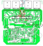
That is provision to use SMT ceramic caps here, they get in parallel to the big elcos C20 C21. You can see others SMT caps parallel directly to other elcos soldered from the bottom.
I am not sure that position for those two is good, maybe better to put them directly to the elcos.
This is the modification/option discussed by Leach in his Lo Tim articles.Is this an alternative way?
It is very similar to D.Self's diagram.
But the diagram is misleading in that it ignores twisted Pairs, almost as if they did not exist.
It is always worth trying the two options:
RCA input socket Return to MAG (post400)
or
PCB input Signal Return to MAG. (post394)
But,
BEFORE experimenting with these alternatives you MUST sort ALL the Flow and Return close coupled (or twisted) Pairs.
Last edited:
HF decoupling.Another question. What are these caps? They are not in the schematic.
This is the best way to lay out an amplifier PCB.
Power +ve and Power -ve beside Power Ground. The power wires arrive as a twisted triplet at the three pads.
Then you can add in the HF decoupling right next to the three pads. The shortest and lowest inductance routes available.
I have bought some 220nF (0.1" pin pitch) and 1uF (805) for this duty.
Tomchr and a few others advocate even larger values for HF decoupling.
H.Ott suggests we buy the highest uF in the package size.
Last edited:
This is the modification/option discussed by Leach in his Lo Tim articles.
It is very similar to D.Self's diagram.
But the diagram is misleading in that it ignores twisted Pairs, almost as if they did not exist.
It is always worth trying the two options:
RCA input socket Return to MAG (post400)
or
PCB input Signal Return to MAG. (post394)
But,
BEFORE experimenting with these alternatives you MUST sort ALL the Flow and Return close coupled (or twisted) Pairs.
Andrew, look this PCB wiring, twisted pairs and twisted triples.
http://www.diyaudio.com/forums/solid-state/182554-thermaltrak-tmc-amp-38.html#post4194947
took me to post401?
I saw and commented on this PCB layout today, that showed the +ve & -ve & PG arriving on the PCB as three close coupled pads.
I said "This is the best way to lay out an amplifier PCB."
It even had HF decoupling (smd) between the close coupled PCB pads.
Well done.
I saw and commented on this PCB layout today, that showed the +ve & -ve & PG arriving on the PCB as three close coupled pads.
I said "This is the best way to lay out an amplifier PCB."
It even had HF decoupling (smd) between the close coupled PCB pads.
Well done.
Last edited:
took me to post401?
I saw and commented on this PCB layout today, that showed the +ve & -ve & PG arriving on the PCB as three close coupled pads.
I said "this is the best way to do it"
It even had HF decoupling (smd) between the close coupled PCB pads.
Well done.
It should be post 372, I don't know why it sometimes doesn't work.
Post374 also shows something that is overlooked in most layouts and amplifier wiring.
Start at the speaker leads.
They are a twisted pair.
They go to close coupled Spkr and SPK Return.
SPK Return passes as a black (hard wire) over the PCB roughly following the centroid of the FLOW currents coming from the output devices. i.e. the Return wire is close coupled to the FLOW routes.
Then the Return attaches to the PG and Returns along the Power cable along with the +ve & -ve FLOW from the PSU.
The transient currents in the SPKR cables are resolved in the close coupled Flow and Return traces and wires.
As I said in opening. This is usually ignored in amplifier wiring.
We generally see long lengths of SINGLE wire going to some remote connection point !!!!!
Someone recently showed a vol pot wired with "grounds" going to a remote connection point and argued that this OPEN LOOP method was OK.
How wrong !
Last edited:

please check here.
That is ISP power ground and goes to the common star ground.
To be clear I added the PCB wiring picture, all black wires go to the common star ground except that one for the speaker.
Attachments
![DADO-TT-TMC-7-2-g-2.LAY].jpg](/community/data/attachments/433/433338-a4b0e94b74915a7412ea7bd152790aac.jpg?hash=pLDpS3SRWn)
Last edited:
Voltage reference wires that do not carry current can be single wires and they can be long/longer.
It's the current carrying wires that must be close coupled to minimise interference effects.
It's the current carrying wires that must be close coupled to minimise interference effects.
But why is it "better" to run long wires to the star rather than a short jumper on the PCB?Voltage reference wires that do not carry current can be single wires and they can be long/longer.
It's the current carrying wires that must be close coupled to minimise interference effects.
It should be post 372, I don't know why it sometimes doesn't work.
It does for me. And Andrew's 374 is, I presume, 346 on my screen.
Because power GND is a dirty GNDBut why is it "better" to run long wires to the star rather than a short jumper on the PCB?
Ok it is more clear nowThat is ISP power ground and goes to the common star ground.
To be clear I added the PCB wiring picture, all black wires go to the common star ground except that one for the speaker.
- Status
- Not open for further replies.
- Home
- Amplifiers
- Solid State
- ThermalTrak+TMC amp