Still to big, or my screen is to small (I use a laptop) or your (screen) is to big.
I have a cheap Acer widescreen laptop. So my screen is small.
Have you any hints on what can be done better?
")
Paul
I have a cheap Acer widescreen laptop. So my screen is small.
Have you any hints on what can be done better?
Paul
I am not sure. I use IrfanView free software to paste clipboard images. For the Waveforms use grid, much easier to follow the values.
Damir
Have you any hints on what can be done better?
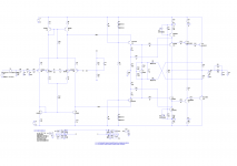
I found the second, smaller attachment a convenient size
The readability can be fixed if you don't use JPG, this is a lossy compression optimised for photos.
PNG should work better.
I have a few ideas on the compensation, I will play around and we can experiment.
Best wishes
David
I found the second, smaller attachment a convenient size
The readability can be fixed if you don't use JPG, this is a lossy compression optimised for photos.
PNG should work better.
I use Bullzip PDF printer. It has many formats. I shall try PNG type files.
I have a few ideas on the compensation, I will play around and we can experiment.
Best wishes
David
Hi David,
Sounds interesting. I shall build a prototype (less compensation). Got the next three days off work so should have plenty of time to experiment.
Are you like me in that you find compensation of an amp a very interesting area of study.
Thank you for your interest in this amplifier.
One side thought. I wonder if you could use the supertis front end as part of class I style output stage.
Paul
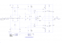
Edit: This image any better?
Attachments
Last edited:
...I wonder if you could use the supertis front end as part of class I style output...
Probably, but I don't see the point.
Optimised compensation can already achieve PPM distortion from an amp of essentially the same complexity as your prototype.
That's why I am interested in compensation
But there is remarkably little about rational optimisation, just handed down "wisdom" on what someone was (or wasn't) able to make work, of limited application outside their specific situation.
Firstly, don't be diffident about a compensation scheme that is "only" an overall loop compensation with no TMC or OIC tricks.
Theory says this should work best of all, if the characteristics of the open loop, uncompensated amplifier allow it.
Secondly, you say "The amp seems to want to run fast. If you slow it down all the compensation looks sub-optimal" and I think you should not be hesitant here either.
I believe it should be possible to push the ULGF up. Most of the rules of thumb come from sub-optimal layouts, and often old, slow transistors.
Best practice I am aware of is Ovidiu Poppa at 6 or 7 MHz, so if that's what the answer comes out then I say try it!
Of course, that's easy for me to say, when it's you who build the prototype.
But I do plan to try this myself, maybe time to order another batch of Thermal Trak output transistors.
The maximum theoretical ULGF is limited by the open loop response of the amplifier.
Bode discusses this, it looks simple, in fact simple proportion.
An amp with gain that drops to 1 and (say) a two pole response at 10 MHz, can be used at 5 MHz with a one pole response (90 PM).
And proportionally with other PM.
But your schematic made me realize that I don't understand exactly how this is modified by a zero in the feedback network (so called phantom zero because it does not require any improvements in the forward gain).
There's a few articles about this in IEEE on-line journals, I need to visit the library for this because I have no access from home.
Will do tomorrow.
...any better?
Yes, it's adequate on my monitor
Best wishes
David
Last edited:
Lunchtime experimentation
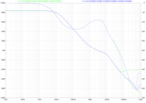
Been messing again with the compensation. Two pole bootstrapped shunts on the VAS outputs. The difference in loop gain plots is significant. But then so is the stability (as expected). Looks much like a CFA loop gain plot.
The prototype is on its way... Sometime this week it will be ready for testing. Going for a higher ULGF than normal @3MHz. Then if this works I may try implementing the attached....
Paul
Attachments
Looks correct to me.
The simple probe placed where I recommended, at the bases of the input transistors, should return essentially the same result as the differential probe where you already have it, for the VAS, with the compensation you have.
This will be a useful cross-check, which I claim as my excuse for why I didn't immediately see this last nite.
Exactly what to call the compensation is a bit less clear.
I don't see it as close to TMC (not "transitional") or OIC (which I define as Miller compensation from the OPS back to the VAS).
It is a Two Pole (to use the term loosely) overall loop with some shunt compensation.
Best wishes
David
Hi David
I showed this compensation over a 1 1/2 ago on my current feedback designs and mentioned some os its benefits. Its indeed called 2 pole shunt compensation, and consits of two independant shunts either to ground or the rails. Its interesting to compare it to the more conventional 2 pole compensation. Damir has in some of his designs added some feedback from the outputstage to this which gives surprisingly good results.
New Years Update
Happy New Year.
Been busy this past few days. Catching up with this project.
The previous versions have all been built. All worked as expected once a few tweaks had been made to ensure that the sims vaguley reflected real life. Then went on a characteristic quest to improve the specs...
David, you said let it run fast well here it is...
(ULGF = 5.6 MHz, PM = 76 degrees, GM = 10dB)
It plays music but not done any specific stability tests yet.
I think I am being held back by the speed of the output devices. Could go with MOSFETs??
Further developments to this project will include a DC Servo and maybe an autobias scheme.
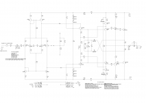
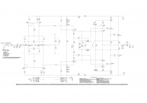
What do people think? Here are some attachments. The .asc is the current prototype.
Paul
Happy New Year.
Been busy this past few days. Catching up with this project.
The previous versions have all been built. All worked as expected once a few tweaks had been made to ensure that the sims vaguley reflected real life. Then went on a characteristic quest to improve the specs...
David, you said let it run fast
well here it is... (ULGF = 5.6 MHz, PM = 76 degrees, GM = 10dB)
It plays music but not done any specific stability tests yet.
I think I am being held back by the speed of the output devices. Could go with MOSFETs??
Further developments to this project will include a DC Servo and maybe an autobias scheme.
What do people think? Here are some attachments. The .asc is the current prototype.
Paul
Attachments
Last edited:
Happy New Year.
Been busy this past few days. Catching up with this project.
The previous versions have all been built. All worked as expected once a few tweaks had been made to ensure that the sims vaguley reflected real life. Then went on a characteristic quest to improve the specs...
David, you said let it run fast
(ULGF = 5.6 MHz, PM = 76 degrees, GM = 10dB)
It plays music but not done any specific stability tests yet.
I think I am being held back by the speed of the output devices. Could go with MOSFETs??
Further developments to this project will include a DC Servo and maybe an autobias scheme.
What do people think? Here are some attachments. The .asc is the current prototype.
Paul
Hi Paul,
Very interesting, I did not try to simulate it yet. You have actually built it? So, high ULGF is not a problem?
My CFA mosfet amp has very similar ULGF (4.1MHz) and LG (75dB up to 20kHz a bit better PM and GM), and just in a process to be built.
Happy New Year
Damir
Hi Paul,
Very interesting, I did not try to simulate it yet. You have actually built it? So, high ULGF is not a problem?
My CFA mosfet amp has very similar ULGF (4.1MHz) and LG (75dB up to 20kHz a bit better PM and GM), and just in a process to be built.
Happy New Year
Damir
Hi Damir,
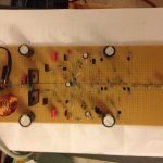
Yes, this is a working prototype. All built on vero board. No signs of oscillations on the scope yet. Sure to find something.
The high ULGF does not seem a problem. Even with the most compromised layout possible. Just trying to think of ways to make this circuit faster so I have the stability margins to play with when trying for 6MHz.
Look forward to the completion of your CFA.
Paul
Attachments
Last edited:
Hi Paul
Compliments of the season. Nice to see the prototype.
Yes, if it works tolerably well with that veroboard then a proper optimized layout should have plenty of room for improvement.
Quite a reassurance.
You can use capacitors to bypass the current mirror emitter resistors R8 and it's complement R10.
Similarly capacitors to bypass the LTP emitter resistors R2,R3 and complement.
This can be one capacitor from one emitter of the LTP to the other (Q1 to Q3 etc.).
Best wishes
David
Compliments of the season. Nice to see the prototype.
...does not seem a problem. Even with the most compromised layout possible.
Yes, if it works tolerably well with that veroboard then a proper optimized layout should have plenty of room for improvement.
Quite a reassurance.
...to think of ways to make this circuit faster so I have the stability...
You can use capacitors to bypass the current mirror emitter resistors R8 and it's complement R10.
Similarly capacitors to bypass the LTP emitter resistors R2,R3 and complement.
This can be one capacitor from one emitter of the LTP to the other (Q1 to Q3 etc.).
Best wishes
David
Last edited:
Been messing again with the compensation. Two pole bootstrapped shunts on the VAS outputs. The difference in loop gain plots is significant. But then so is the stability (as expected). Looks much like a CFA loop gain plot.
The prototype is on its way... Sometime this week it will be ready for testing. Going for a higher ULGF than normal @3MHz. Then if this works I may try implementing the attached....
Paul
Your output stage is same as mine.
What do you think about this output stage? Better than EF3?
Hi Paul
Compliments of the season. Nice to see the prototype.
Yes, if it works tolerably well with that veroboard then a proper optimized layout should have plenty of room for improvement.
Quite a reassurance.
Hi David,
I always do my prototypes on vero board with component layout as per schematic. That way if I can get it stable in that form then I have a real chance of successfully creating a proper PCB.
The other factor is that I spent a lot of money on my first design which didn't really work properly. Not making that same mistake again. That was done straight to PCB with no prototype.
You can use capacitors to bypass the current mirror emitter resistors R8 and it's complement R10.
Similarly capacitors to bypass the LTP emitter resistors R2,R3 and complement.
This can be one capacitor from one emitter of the LTP to the other (Q1 to Q3 etc.).
Best wishes
David
These ideas work. Have managed to improve stability margins a little while increasing the ULGF to 6MHz. Shall continue playing with the compensation. Sure there's more to come.
Keep thinking about going back to MOSFETs with a push /pull driver stage?
Thank you again for your help
Paul
Hi Bimo,
In this particular instance I like the OPS with the current source / inverted pre-driver. The VAS used in this amp is highly sensitive to non linear capacitive loading. So by using this pre driver configuration this problem is reduced. Another small advantage is that two of the Vbe drops cancel. Can get closer to the rails.
I just chose to drive the collectors of the Pre Drivers from the amp output as an alternative to the diamond buffer OPS. Which Im not convinced is fully stable with additional precautions taken.
At the moment I'm staying away from the 3EF. Not had any meaningful experience with it. I'd rather spend my time with an inverted (Class A) CFP driver (+CCS) + EF Output devices. Where the EF is a pair of MOSFETs.
Paul
You can use capacitors to bypass the current mirror emitter resistors R8 and it's complement R10.
Similarly capacitors to bypass the LTP emitter resistors R2,R3 and complement.
This can be one capacitor from one emitter of the LTP to the other (Q1 to Q3 etc.).
Best wishes
David
Hi David,
Been experimenting with this and have found that it is trading GM for PM. Have been using capacitor values of the order of 22pF to 390pF. Is this the expected behaviour?
Also, interestingly changing Q14 and Q15 (predrivers) has a significant affect on the stability parameters (ULGF, LG, PM, GM). Is this down to transistor models? Or are there specific requirements for the transistors in these places?
Even slightly changing the output stage topology slightly has an affect. If you feed the collectors of the pre drivers from the power rails things improve.
All interesting stuff... (at least for me
)More factors at play than I am aware of...
Paul
6MHz....
Hi All,
The ULGF is now 6.5Mhz (ish). PM = 82 degrees, GM = 11dB. Managed to improve the stability as well as upping the ULGF.
It is pretty stable. Plays music nicely. Clipping behaviour is almost exactly as expected. Square waves are clean with no overshoot. This was probed at the amp output before the output filter while connected to speaker.
All this on strip board with a poor earthing arrangement.
Is it worth pushing for a higher ULGF? It can be done in Spice. Suppose I need to define some stability tests. It happily drives a KEF Coda 7.
The only difference between the .asc file is the use of KSA733/KSC945 (Q14,Q15) in the prototype instead of KSA992/KSC1815. Don't have reliable models for the transistors used. Maybe I should try and learn how to make Spice models.
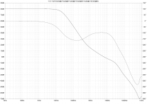
Attached are the schematic, LG plot and .asc
Many thanks for reading this thread.
Paul
Hi All,
The ULGF is now 6.5Mhz (ish). PM = 82 degrees, GM = 11dB. Managed to improve the stability as well as upping the ULGF.
It is pretty stable. Plays music nicely. Clipping behaviour is almost exactly as expected. Square waves are clean with no overshoot. This was probed at the amp output before the output filter while connected to speaker.
All this on strip board with a poor earthing arrangement.
Is it worth pushing for a higher ULGF? It can be done in Spice. Suppose I need to define some stability tests. It happily drives a KEF Coda 7.
The only difference between the .asc file is the use of KSA733/KSC945 (Q14,Q15) in the prototype instead of KSA992/KSC1815. Don't have reliable models for the transistors used. Maybe I should try and learn how to make Spice models.
Attached are the schematic, LG plot and .asc
Many thanks for reading this thread.
Paul
Attachments
Last edited:
...I always do my prototypes on vero board with component layout as per schematic...
I like the idea of a prototype but I don't think you need to layout as per schematic.
To simplistically copy the schematic usually leads to sub-optimal layout, but it's such an obvious way that most people tend to do it, even for the PCB.
Of course, you could say that if a circuit can cope with Vero-board AND sub-optimal layout then it will be VERY likely to work on optimised PCB.
But I would say, may as well at least start to consider layout.
...back to MOSFETs with a push /pull driver ...
No doubt feasible but, in my view, not worth the other compromises.
Lower efficiency from the typically increased MOSFET bias and extra rail headroom needed, a bit extra complexity, MOSFET capacitance modulation.
...trad[es] GM for PM. Have been using capacitor values of the order of 22pF to 390pF. Is this the expected behaviour?
It is typical, but it's not zero-sum because it is possible to substantially improve PM while the loss of GM is minimal.
It is easiest to see this on a Nichols plot.
Still haven't worked out how to make LTSpice do this neatly, in the meantime you can look at the chart to see how they trade-off.
... Q14 and Q15 (predrivers) has a significant affect on the stability parameters (ULGF, LG, PM, GM). Is this down to transistor models? Or are there specific requirements for the transistors in these places?
I was never completely happy with my EF3 results, there are non obvious effects and a tendency to sensitivity, as you have noted.
Dennis Feucht has some discussion of this and some of Middlebrook looks relevant but I decided it was easier to use EF2 and use sufficient feedback around the VAS to make the extra load inconsequential.
Maybe not so simple for your Edmond Stuart style VAS/TIS that is more sensitive to load.
I discussed this a little with Edmond in his thread on the topic.
Extra complexity in the OPS versus simpler OPS but couple extra transistors in the front end.
I am happy with my version of the later but maybe when I understand more I will reconsider.
Best wishes
David
Last edited:
I like the idea of a prototype but I don't think you need to layout as per schematic.
To simplistically copy the schematic usually leads to sub-optimal layout, but it's such an obvious way that most people tend to do it, even for the PCB.
Of course, you could say that if a circuit can cope with Vero-board AND sub-optimal layout then it will be VERY likely to work on optimised PCB.
But I would say, may as well at least start to consider layout.
Hi David,
This is the thinking. If it works on veroboard it is unlikely I'll be wasting my money again on PCBs that don't work.
It also makes it easier on my brain to transfer mods from LTSpice to the prototype.Always have layout in mind while designing. I like to minimise the number of GND connections as these have proved most troublesome for me. Also, I try to imagine how the connections would work on PCB so there are not too many crossings. Like the idea of the Cherry recommendation of running the power rails down the middle of the PCB. That way you can avoid all the sensitive electronics being inbetween the main sources of interference.
Experience was expensive...
Do like the fact it works ok with the ~6MHz ULGF on veroboard.
No doubt feasible but not worth the other compromises to my mind.
Lower efficiency from the typically increased MOSFET bias and extra rail headroom needed, a bit extra complexity, MOSFET capacitance modulation.
Agreed,
The compromises are significant and what is currently a "simple" design would become a relative monster. That is why it got as far as LTSpice and stopped there.
It is typical, but it's not zero-sum because it is possible to substantially improve PM while the loss of GM is minimal.
It is easiest to see this on a Nichols plot.
Still haven't worked out how to make LTSpice do this neatly, in the meantime you can look at the chart to see how they trade-off.
Have to take a closer look. Don't have too much GM to play with...
I was never completely happy with my EF3 results, there are non obvious effects and a tendency to sensitivity, as you have noted.
Dennis Feucht has some discussion of this and some of Middlebrook looks relevant but I decided it was easier to use EF2 and use sufficient feedback around the VAS to make the extra load inconsequential.
Best wishes
David
Always had a fear of the 3EF myself. Maybe could use a CFP for the Pre drivers / drivers?
I thought that the changes in LG (-6db across the band in one case) when the Pre drivers were changed was a feature of the design not the 3EF. In this design it needs the Pre drivers because of the kind of VAS used. It has a very high output impedance. Or at least this is how I understand it with the compensation type used.
Got a significant improvement in THD when going from a 2EF to a 3EF...
Even more research required...
Paul
Last edited:
...Maybe could use a CFP for the Pre drivers / drivers?
I have simulated this and it did not work as well as I expected.
Those expectations were not just hope but based on simple theory, apparently TOO simple.
The unexpected bit was a result of source resistance, not revealed if one just tries an OPS driven from an ideal source.
...it needs the Pre drivers because of the kind of VAS used. It has a very high output impedance. Or at least this is how I understand it with the compensation type used.
Yes, I added a few comments about this after I pushed "submit" so we cross posted.
I try to put the posts up quickly but went a bit early.
Best wishes
David
- Status
- This old topic is closed. If you want to reopen this topic, contact a moderator using the "Report Post" button.
- Home
- Amplifiers
- Solid State
- Amp designed during lunch breaks